Deck 11: JFETS
Full screen (f)
Question
Question
Question
Question
Question
Question
Question
Question
Question
Question
Question
Question
Question
Question
Question
Question
Question
Question
Question
Question
Question
Question
Question
Question
Question
Question
Question
What is the breakdown voltage as listed on the drain curves shown in Figure 11-5? 
A) 0 V
B) 4 V
C) 15 V
D) 30 V
A) 0 V
B) 4 V
C) 15 V
D) 30 V
Question
Question
Question
What is the pinchoff voltage as listed on the drain curves shown in Figure 11-5? 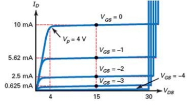
A) 0 V
B) - 1 V
C) 15 V
D) 4 V
A) 0 V
B) - 1 V
C) 15 V
D) 4 V
Question
Question
Question
Question
Question
Question
Question
Question
Question
Question
Question
Question
Question
Question
Question
Question
Question
Question
Question
Question

Unlock Deck
Sign up to unlock the cards in this deck!
Unlock Deck
Unlock Deck
1/50
Play
Full screen (f)
Deck 11: JFETS
1
The transconductance curve of a JFET is a graph of drain current versus voltage gate to source.
True
2
The JFET is a voltage-controlled device because an input voltage controls an output current.
True
3
What is a circuit that steers one or more of the input signals to the output line?
A) dc amplifier
B) regulator
C) oscillator
D) multiplexer
A) dc amplifier
B) regulator
C) oscillator
D) multiplexer
D
4
In order to produce a JFET,a manufacturer diffuses two areas of p-type semiconductor into the n-type semiconductor.
Unlock Deck
Unlock for access to all 50 flashcards in this deck.
Unlock Deck
k this deck
5
A stage that isolates the preceding stage from the following stage is called a
A) chopper amplifier.
B) driver amplifier.
C) buffer amplifier.
D) preamplifier.
A) chopper amplifier.
B) driver amplifier.
C) buffer amplifier.
D) preamplifier.
Unlock Deck
Unlock for access to all 50 flashcards in this deck.
Unlock Deck
k this deck
6
In the schematic symbol for a p-channel JFET,the gate arrow points out.
Unlock Deck
Unlock for access to all 50 flashcards in this deck.
Unlock Deck
k this deck
7
A slow shift in the final dc output voltage produced by minor changes in supply voltage,transistor parameters,and temperature variations is referred to as _________.
A) drift
B) transconductance
C) pinchoff
D) chopper
A) drift
B) transconductance
C) pinchoff
D) chopper
Unlock Deck
Unlock for access to all 50 flashcards in this deck.
Unlock Deck
k this deck
8
Circuits that amplify frequencies down to 0 Hz are called
A) small-signal amplifiers.
B) narrowband amplifiers.
C) dc amplifiers.
D)tuned RF amplifiers.
A) small-signal amplifiers.
B) narrowband amplifiers.
C) dc amplifiers.
D)tuned RF amplifiers.
Unlock Deck
Unlock for access to all 50 flashcards in this deck.
Unlock Deck
k this deck
9
The current drain to source with a shorted gate (IDSS )is the maximum drain current a JFET can produce.
Unlock Deck
Unlock for access to all 50 flashcards in this deck.
Unlock Deck
k this deck
10
Gate bias is the best way to bias a JFET in the active region because the Q point is very stable.
Unlock Deck
Unlock for access to all 50 flashcards in this deck.
Unlock Deck
k this deck
11
A JFET chopper can be used to build a dc amplifier.
Unlock Deck
Unlock for access to all 50 flashcards in this deck.
Unlock Deck
k this deck
12
A circuit that generates an ac signal is
A) a rectifier.
B) an oscillator.
C) an oscilloscope.
D) a channel.
A) a rectifier.
B) an oscillator.
C) an oscilloscope.
D) a channel.
Unlock Deck
Unlock for access to all 50 flashcards in this deck.
Unlock Deck
k this deck
13
A JFET common-source amplifier produces a noninverted output that is coupled from the drain.
Unlock Deck
Unlock for access to all 50 flashcards in this deck.
Unlock Deck
k this deck
14
Transconductance tells us how effective the gate-source voltage is in controlling the source current.
Unlock Deck
Unlock for access to all 50 flashcards in this deck.
Unlock Deck
k this deck
15
The unit mho is the ratio of current to voltage and the modern unit for mho is the siemen.
Unlock Deck
Unlock for access to all 50 flashcards in this deck.
Unlock Deck
k this deck
16
The supply voltage (VDD )for a JFET forces free electrons to flow from the drain to the source.
Unlock Deck
Unlock for access to all 50 flashcards in this deck.
Unlock Deck
k this deck
17
JFET self-bias results when the circuit creates its own bias by using the voltage developed across the source resistor to reverse-bias the gate.
Unlock Deck
Unlock for access to all 50 flashcards in this deck.
Unlock Deck
k this deck
18
A JFET analog switch operates either in the ohmic region or in the cutoff region.
Unlock Deck
Unlock for access to all 50 flashcards in this deck.
Unlock Deck
k this deck
19
The source and drain terminals are interchangeable at high frequencies.
Unlock Deck
Unlock for access to all 50 flashcards in this deck.
Unlock Deck
k this deck
20
The term field effect is related to the depletion layers around each p region of a JFET.
Unlock Deck
Unlock for access to all 50 flashcards in this deck.
Unlock Deck
k this deck
21
Which amplifying device is preferred for most linear applications?
A) FET
B) BJT
C) triode
D) magnetron
A) FET
B) BJT
C) triode
D) magnetron
Unlock Deck
Unlock for access to all 50 flashcards in this deck.
Unlock Deck
k this deck
22
The almost-vertical part of the drain curve below pinchoff is called the
A) static region.
B) channel.
C) ohmic region.
D) saturation.
A) static region.
B) channel.
C) ohmic region.
D) saturation.
Unlock Deck
Unlock for access to all 50 flashcards in this deck.
Unlock Deck
k this deck
23
The minimum JFET voltage VP is called
A) cutoff voltage.
B) filtered voltage.
C) reverse voltage.
D) pinchoff voltage.
A) cutoff voltage.
B) filtered voltage.
C) reverse voltage.
D) pinchoff voltage.
Unlock Deck
Unlock for access to all 50 flashcards in this deck.
Unlock Deck
k this deck
24
In audio applications,JFETs are often used as
A) analog switches.
B) tuned RF amplifiers.
C) common-source amplifiers.
D) source followers.
A) analog switches.
B) tuned RF amplifiers.
C) common-source amplifiers.
D) source followers.
Unlock Deck
Unlock for access to all 50 flashcards in this deck.
Unlock Deck
k this deck
25
The power supply for a JFET forces free electrons to flow from
A) drain to source.
B) source to drain.
C) gate to source.
D) gate to drain.
A) drain to source.
B) source to drain.
C) gate to source.
D) gate to drain.
Unlock Deck
Unlock for access to all 50 flashcards in this deck.
Unlock Deck
k this deck
26
The JFET is a
A) voltage-controlled device.
B) current-controlled device.
C) bipolar device.
D) nonlinear device.
A) voltage-controlled device.
B) current-controlled device.
C) bipolar device.
D) nonlinear device.
Unlock Deck
Unlock for access to all 50 flashcards in this deck.
Unlock Deck
k this deck
27
What is the breakdown voltage as listed on the drain curves shown in Figure 11-5?
A) 0 V
B) 4 V
C) 15 V
D) 30 V
A) 0 V
B) 4 V
C) 15 V
D) 30 V
Unlock Deck
Unlock for access to all 50 flashcards in this deck.
Unlock Deck
k this deck
28
Which instrument cannot be used in the testing of a JFET?
A) curve tracer
B) oscilloscope
C) watt meter
D) DMM
A) curve tracer
B) oscilloscope
C) watt meter
D) DMM
Unlock Deck
Unlock for access to all 50 flashcards in this deck.
Unlock Deck
k this deck
29
Because of the large spread in JFET parameters,which method of biasing cannot be used?
A) gate
B) VDB
C) two supply
D) current source
A) gate
B) VDB
C) two supply
D) current source
Unlock Deck
Unlock for access to all 50 flashcards in this deck.
Unlock Deck
k this deck
30
What is the pinchoff voltage as listed on the drain curves shown in Figure 11-5?
A) 0 V
B) - 1 V
C) 15 V
D) 4 V
A) 0 V
B) - 1 V
C) 15 V
D) 4 V
Unlock Deck
Unlock for access to all 50 flashcards in this deck.
Unlock Deck
k this deck
31
A graph of drain current versus voltage gate to source is called
A) drain curve.
B) transconductance curve.
C) gate curve.
D) conductance curve.
A) drain curve.
B) transconductance curve.
C) gate curve.
D) conductance curve.
Unlock Deck
Unlock for access to all 50 flashcards in this deck.
Unlock Deck
k this deck
32
To prevent unwanted changes in volume,most modern receivers use
A) automatic frequency control.
B) automatic gain control.
C) faders.
D) woofers.
A) automatic frequency control.
B) automatic gain control.
C) faders.
D) woofers.
Unlock Deck
Unlock for access to all 50 flashcards in this deck.
Unlock Deck
k this deck
33
An entry shown on the data sheet that helps to determine the dc input resistance of a JFET is _________.
A) IGSS
B) VGS
C) ID
D) RS
A) IGSS
B) VGS
C) ID
D) RS
Unlock Deck
Unlock for access to all 50 flashcards in this deck.
Unlock Deck
k this deck
34
The current flowing from the JFET's source to drain must pass through what between the depletion layers?
A) gate
B) ground
C) channel
D) base
A) gate
B) ground
C) channel
D) base
Unlock Deck
Unlock for access to all 50 flashcards in this deck.
Unlock Deck
k this deck
35
The source and drain terminals are
A) changeable at high frequencies.
B) not changeable at high frequencies.
C) not changeable at low frequencies.
D) connected to the gate.
A) changeable at high frequencies.
B) not changeable at high frequencies.
C) not changeable at low frequencies.
D) connected to the gate.
Unlock Deck
Unlock for access to all 50 flashcards in this deck.
Unlock Deck
k this deck
36
A typical JFET has an input resistance of
A) about 200 ohms.
B) about 2000 ohms.
C) about 200 kΩ.
D) about 200 MΩ.
A) about 200 ohms.
B) about 2000 ohms.
C) about 200 kΩ.
D) about 200 MΩ.
Unlock Deck
Unlock for access to all 50 flashcards in this deck.
Unlock Deck
k this deck
37
With a JFET,the gate-source diode is
A) always reverse-biased.
B) always forward-biased.
C) is connected to the drain voltage.
D) is connected to ground.
A) always reverse-biased.
B) always forward-biased.
C) is connected to the drain voltage.
D) is connected to ground.
Unlock Deck
Unlock for access to all 50 flashcards in this deck.
Unlock Deck
k this deck
38
A JFET is a symmetrical device at low frequencies since
A) either end can act like a source or the drain.
B) either end can act like a source or the gate.
C) either end can act like a drain or the gate.
D) either end can act like the channel.
A) either end can act like a source or the drain.
B) either end can act like a source or the gate.
C) either end can act like a drain or the gate.
D) either end can act like the channel.
Unlock Deck
Unlock for access to all 50 flashcards in this deck.
Unlock Deck
k this deck
39
Since the field-effect transistor depends on only one type of charge,it is referred to as _________.
A) unipolar
B) bipolar
C) singular
D) unilateral
A) unipolar
B) bipolar
C) singular
D) unilateral
Unlock Deck
Unlock for access to all 50 flashcards in this deck.
Unlock Deck
k this deck
40
One of the most important pieces of information on the data sheet of a depletion-mode device is
A) derating factor.
B) reverse breakdown.
C) maximum drain current.
D) minimum gate to source voltage.
A) derating factor.
B) reverse breakdown.
C) maximum drain current.
D) minimum gate to source voltage.
Unlock Deck
Unlock for access to all 50 flashcards in this deck.
Unlock Deck
k this deck
41
What is the type of JFET circuit that has the ac signal coupled to the gate and the output taken from the drain?
A) common source
B) common drain
C) common gate
D) source follower
A) common source
B) common drain
C) common gate
D) source follower
Unlock Deck
Unlock for access to all 50 flashcards in this deck.
Unlock Deck
k this deck
42
Which JFET amplifier configuration exhibits a very high input impedance and low output impedance?
A) common source
B) common gate
C) source follower
D) drain follower
A) common source
B) common gate
C) source follower
D) drain follower
Unlock Deck
Unlock for access to all 50 flashcards in this deck.
Unlock Deck
k this deck
43
How effective the gate-source voltage is controlling the drain current is referred to as _________.
A) pinchoff
B) saturation
C) transconductance
D) conductance
A) pinchoff
B) saturation
C) transconductance
D) conductance
Unlock Deck
Unlock for access to all 50 flashcards in this deck.
Unlock Deck
k this deck
44
What is unwanted disturbance superimposed on a useful signal?
A) alternating current
B) harmonics
C) chassis
D) noise
A) alternating current
B) harmonics
C) chassis
D) noise
Unlock Deck
Unlock for access to all 50 flashcards in this deck.
Unlock Deck
k this deck
45
A JFET circuit that converts a dc input voltage to a square-wave output is
A) a regulator.
B) a chopper.
C) an inverter.
D) a rectifier.
A) a regulator.
B) a chopper.
C) an inverter.
D) a rectifier.
Unlock Deck
Unlock for access to all 50 flashcards in this deck.
Unlock Deck
k this deck
46
What is the equivalent and modern unit for mho?
A) ohm
B) farad
C) siemen
D) henry
A) ohm
B) farad
C) siemen
D) henry
Unlock Deck
Unlock for access to all 50 flashcards in this deck.
Unlock Deck
k this deck
47
Why is gate bias the worst method to bias a JFET in the active region?
A) because the operating point is too unstable
B) because the operating point is too stable
C) because the Q point is at pinchoff
D) because the gate is forward biased
A) because the operating point is too unstable
B) because the operating point is too stable
C) because the Q point is at pinchoff
D) because the gate is forward biased
Unlock Deck
Unlock for access to all 50 flashcards in this deck.
Unlock Deck
k this deck
48
Self-biasing a JFET is used only with
A) small-signal amplifiers.
B) power amplifiers.
C) wideband amplifiers.
D) tuned RF amplifiers.
A) small-signal amplifiers.
B) power amplifiers.
C) wideband amplifiers.
D) tuned RF amplifiers.
Unlock Deck
Unlock for access to all 50 flashcards in this deck.
Unlock Deck
k this deck
49
The JFET source follower has
A) low input resistance.
B) high voltage gain.
C) a voltage gain less than one.
D) the output taken from the drain.
A) low input resistance.
B) high voltage gain.
C) a voltage gain less than one.
D) the output taken from the drain.
Unlock Deck
Unlock for access to all 50 flashcards in this deck.
Unlock Deck
k this deck
50
When the JFET operates in only the ohmic region or in the cutoff region,it is being used as
A) an analog switch.
B) a linear amplifier.
C) an oscillator.
D) a regulator.
A) an analog switch.
B) a linear amplifier.
C) an oscillator.
D) a regulator.
Unlock Deck
Unlock for access to all 50 flashcards in this deck.
Unlock Deck
k this deck
Unlock Deck
Unlock for access to all 50 flashcards in this deck.


