Deck 6: BJT Fumdamentals
Full screen (f)
Question
Question
Question
Question
Question
Question
Question
Question
Question
Question
Question
Question
Question
Question
Question
Question
Question
Question
Question
Question
Question
Question
Question
Question
Question
Question
Question
Question
Question
Question
What type transistor connection is shown in Figure 6-7 (a)? 
A) common emitter
B) common collector
C) common base
D) emitter follower
A) common emitter
B) common collector
C) common base
D) emitter follower
Question
Question
Question
Question
Question
Question
Question
Question
What is the purpose of RB in the circuit shown in Figure 6-7 (a)? 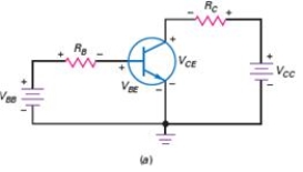
A) load resistor
B) filtering
C) limit current
D) amplify VBB
A) load resistor
B) filtering
C) limit current
D) amplify VBB
Question
Question
What is the source of bias for the transistor's emitter diode shown in Figure 6-7 (a)? 
A) VCC
B) VBB
C) VCE
D) RC
A) VCC
B) VBB
C) VCE
D) RC
Question
Question
Question
Question
Question
Question
Question
What is the possible problem if B is equal to 15 V and C is equal to 15 V? 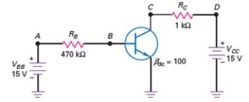
A) transistor is blown open
B) VBB is 0 V
C) transistor is shorted
D) VCC is 0 V
A) transistor is blown open
B) VBB is 0 V
C) transistor is shorted
D) VCC is 0 V
Question
What is the possible problem if B is equal to 0 V and C is equal to 15 V? 
A) transistor is shorted
B) RB is open
C) VCC is 0 V
D) transistor is blown open
A) transistor is shorted
B) RB is open
C) VCC is 0 V
D) transistor is blown open
Question
Question

Unlock Deck
Sign up to unlock the cards in this deck!
Unlock Deck
Unlock Deck
1/50
Play
Full screen (f)
Deck 6: BJT Fumdamentals
1
The dc beta is also known as the current gain because a small base current controls a much larger collector current.
True
2
The middle region of a transistor is the ________.
A) collector
B) emitter
C) base
D) beta
A) collector
B) emitter
C) base
D) beta
C
3
Which region of the transistor is physically the largest?
A) collector
B) emitter
C) base
D) beta
A) collector
B) emitter
C) base
D) beta
A
4
The emitter current in a bipolar junction transistor is equal to the sum of the collector and base currents.
Unlock Deck
Unlock for access to all 50 flashcards in this deck.
Unlock Deck
k this deck
5
The power rating of a transistor can be increased by using a heat sink.
Unlock Deck
Unlock for access to all 50 flashcards in this deck.
Unlock Deck
k this deck
6
When the ground side of each voltage source is connected to the emitter of a bipolar junction transistor,it is called a common collector.
Unlock Deck
Unlock for access to all 50 flashcards in this deck.
Unlock Deck
k this deck
7
The two junctions of a transistor are between the emitter and the base and between the
A) collector and emitter.
B) collector and base.
C) collector and beta.
D) base and committer.
A) collector and emitter.
B) collector and base.
C) collector and beta.
D) base and committer.
Unlock Deck
Unlock for access to all 50 flashcards in this deck.
Unlock Deck
k this deck
8
An unbiased transistor is like two back-to-back diodes.
Unlock Deck
Unlock for access to all 50 flashcards in this deck.
Unlock Deck
k this deck
9
What is the semiconductor material generally used in the manufacturing process of transistors?
A) gallium
B) boron
C) copper
D) silicon
A) gallium
B) boron
C) copper
D) silicon
Unlock Deck
Unlock for access to all 50 flashcards in this deck.
Unlock Deck
k this deck
10
In a system of analysis called h parameters,hFE is defined as the symbol for thermal resistance.
Unlock Deck
Unlock for access to all 50 flashcards in this deck.
Unlock Deck
k this deck
11
A bipolar junction transistor has two doped regions.
Unlock Deck
Unlock for access to all 50 flashcards in this deck.
Unlock Deck
k this deck
12
An unbiased transistor is like
A) a biased diode.
B) two diodes connected in parallel.
C) two back-to-back diodes.
D) two diodes connected in series with a capacitor.
A) a biased diode.
B) two diodes connected in parallel.
C) two back-to-back diodes.
D) two diodes connected in series with a capacitor.
Unlock Deck
Unlock for access to all 50 flashcards in this deck.
Unlock Deck
k this deck
13
Transistor saturation and cutoff regions are useful in digital and computer circuits referred to as switching circuits.
Unlock Deck
Unlock for access to all 50 flashcards in this deck.
Unlock Deck
k this deck
14
In an npn transistor,the emitter and collector are both n-type materials.
Unlock Deck
Unlock for access to all 50 flashcards in this deck.
Unlock Deck
k this deck
15
When double-subscript notations are used and they are the same,the voltage represents a source.
Unlock Deck
Unlock for access to all 50 flashcards in this deck.
Unlock Deck
k this deck
16
Small-signal transistors can dissipate less than 1 watt.
Unlock Deck
Unlock for access to all 50 flashcards in this deck.
Unlock Deck
k this deck
17
A bipolar junction transistor should always operate in the breakdown region.
Unlock Deck
Unlock for access to all 50 flashcards in this deck.
Unlock Deck
k this deck
18
The emitter of a bipolar junction transistor is lightly doped and the base is heavily doped.
Unlock Deck
Unlock for access to all 50 flashcards in this deck.
Unlock Deck
k this deck
19
Surface-mount transistors are generally found in a simple three-terminal,gull-wing package.
Unlock Deck
Unlock for access to all 50 flashcards in this deck.
Unlock Deck
k this deck
20
The dc beta is defined as the dc collector current divided by the dc emitter current.
Unlock Deck
Unlock for access to all 50 flashcards in this deck.
Unlock Deck
k this deck
21
Transistors operate in the active,or linear region when they are used
A) as switching circuits.
B) to amplify weak signals.
C) as rectifiers.
D) in the breakdown region.
A) as switching circuits.
B) to amplify weak signals.
C) as rectifiers.
D) in the breakdown region.
Unlock Deck
Unlock for access to all 50 flashcards in this deck.
Unlock Deck
k this deck
22
On the set of collector curves,the horizontal part of the curve where the collector current is constant,is known as the
A) active region.
B) breakdown region.
C) saturation region.
D) cut-off region.
A) active region.
B) breakdown region.
C) saturation region.
D) cut-off region.
Unlock Deck
Unlock for access to all 50 flashcards in this deck.
Unlock Deck
k this deck
23
The bulk resistance of the emitter diode becomes important
A) in low-power applications only.
B) in high-power applications only.
C) in low-frequency applications only.
D) in high-frequency applications only.
A) in low-power applications only.
B) in high-power applications only.
C) in low-frequency applications only.
D) in high-frequency applications only.
Unlock Deck
Unlock for access to all 50 flashcards in this deck.
Unlock Deck
k this deck
24
When calculating base current for a germanium transistor circuit,the voltage base to emitter is approximated at ________.
A) 0.3 V
B) 0.7 V
C) 1.3 V
D) 1.7 V
A) 0.3 V
B) 0.7 V
C) 1.3 V
D) 1.7 V
Unlock Deck
Unlock for access to all 50 flashcards in this deck.
Unlock Deck
k this deck
25
If the data sheet maximum rating,collector-emitter breakdown voltage is exceeded
A) current gain becomes maximum.
B) the emitter will become reverse biased.
C) the transistor will go into cut-off.
D) the transistor will breakdown and will probably be destroyed.
A) current gain becomes maximum.
B) the emitter will become reverse biased.
C) the transistor will go into cut-off.
D) the transistor will breakdown and will probably be destroyed.
Unlock Deck
Unlock for access to all 50 flashcards in this deck.
Unlock Deck
k this deck
26
Generally,power transistors can dissipate
A) less than 1 W.
B) more than 1 W.
C) more than 100 W.
D) less than 1 mW.
A) less than 1 W.
B) more than 1 W.
C) more than 100 W.
D) less than 1 mW.
Unlock Deck
Unlock for access to all 50 flashcards in this deck.
Unlock Deck
k this deck
27
Kirchoff's current law describes transistor currents as follows:
A) emitter current equals the sum of collector and base currents.
B) collector current equals the sum of base and emitter currents.
C) base current equals the sum of collector and emitter currents.
D) emitter current equals collector current minus the base current.
A) emitter current equals the sum of collector and base currents.
B) collector current equals the sum of base and emitter currents.
C) base current equals the sum of collector and emitter currents.
D) emitter current equals collector current minus the base current.
Unlock Deck
Unlock for access to all 50 flashcards in this deck.
Unlock Deck
k this deck
28
In a common-emitter circuit,once the base current has been calculated,collector current can be determined by multiplying base current by ________.
A) alpha
B) the load resistor
C) maximum power rating
D) beta
A) alpha
B) the load resistor
C) maximum power rating
D) beta
Unlock Deck
Unlock for access to all 50 flashcards in this deck.
Unlock Deck
k this deck
29
High-power transistors (over 1 W)typically have current gains of ________.
A) 1 to 10
B) 10 to 20
C) 20 to 100
D) 100 to 1000
A) 1 to 10
B) 10 to 20
C) 20 to 100
D) 100 to 1000
Unlock Deck
Unlock for access to all 50 flashcards in this deck.
Unlock Deck
k this deck
30
What type transistor connection is shown in Figure 6-7 (a)?
A) common emitter
B) common collector
C) common base
D) emitter follower
A) common emitter
B) common collector
C) common base
D) emitter follower
Unlock Deck
Unlock for access to all 50 flashcards in this deck.
Unlock Deck
k this deck
31
The base region of a transistor is
A) lightly doped and very thick.
B) lightly doped and very thin.
C) heavily doped and very thick.
D) heavily doped and very thin.
A) lightly doped and very thick.
B) lightly doped and very thin.
C) heavily doped and very thick.
D) heavily doped and very thin.
Unlock Deck
Unlock for access to all 50 flashcards in this deck.
Unlock Deck
k this deck
32
An instrument that graphically displays collector current versus the collector to emitter voltage is
A) a voltmeter.
B) a logic probe.
C) an oscilloscope.
D) a curve tracer.
A) a voltmeter.
B) a logic probe.
C) an oscilloscope.
D) a curve tracer.
Unlock Deck
Unlock for access to all 50 flashcards in this deck.
Unlock Deck
k this deck
33
A transistor's current gain is equal to
A) collector current divided by emitter current.
B) emitter current divided by base current.
C) collector current divided by base current.
D) base current divided by collector current.
A) collector current divided by emitter current.
B) emitter current divided by base current.
C) collector current divided by base current.
D) base current divided by collector current.
Unlock Deck
Unlock for access to all 50 flashcards in this deck.
Unlock Deck
k this deck
34
The type of biasing that produces the most useful results is
A) forward-biasing the emitter diode and reverse-biasing the collector diode.
B) reverse-biasing the emitter diode and forward-biasing the collector diode.
C) forward-biasing the collector diode and reverse-biasing the base diode.
D) reverse-biasing the collector diode and forward-biasing the base diode.
Unlock Deck
Unlock for access to all 50 flashcards in this deck.
Unlock Deck
k this deck
35
When working with transistor circuits,single subscripts are used to denote
A) voltage sources.
B) current sources.
C) node voltages.
D) Thevenin's voltages.
A) voltage sources.
B) current sources.
C) node voltages.
D) Thevenin's voltages.
Unlock Deck
Unlock for access to all 50 flashcards in this deck.
Unlock Deck
k this deck
36
When using double-subscript notation with transistor circuits and the subscripts are the same,the voltage represents
A) the voltage between two points.
B) a voltage source.
C) an ac source.
D) the Thevenin's voltage.
A) the voltage between two points.
B) a voltage source.
C) an ac source.
D) the Thevenin's voltage.
Unlock Deck
Unlock for access to all 50 flashcards in this deck.
Unlock Deck
k this deck
37
A transistor has a power dissipation that equals ________.
A) VCE x RC
B) VCE x PD
C) VCE x IC
D) VCE x IB
A) VCE x RC
B) VCE x PD
C) VCE x IC
D) VCE x IB
Unlock Deck
Unlock for access to all 50 flashcards in this deck.
Unlock Deck
k this deck
38
What is the purpose of RB in the circuit shown in Figure 6-7 (a)?
A) load resistor
B) filtering
C) limit current
D) amplify VBB
A) load resistor
B) filtering
C) limit current
D) amplify VBB
Unlock Deck
Unlock for access to all 50 flashcards in this deck.
Unlock Deck
k this deck
39
Transistor saturation and cutoff regions are used in circuits referred to as ________.
A) rectifiers
B) filters
C) switching circuits
D) amplifiers
A) rectifiers
B) filters
C) switching circuits
D) amplifiers
Unlock Deck
Unlock for access to all 50 flashcards in this deck.
Unlock Deck
k this deck
40
What is the source of bias for the transistor's emitter diode shown in Figure 6-7 (a)?
A) VCC
B) VBB
C) VCE
D) RC
A) VCC
B) VBB
C) VCE
D) RC
Unlock Deck
Unlock for access to all 50 flashcards in this deck.
Unlock Deck
k this deck
41
What is the device that increases a transistor's power rating by reducing the internal heat faster?
A) heater wire
B) chassis
C) grommet
D) heat sink
A) heater wire
B) chassis
C) grommet
D) heat sink
Unlock Deck
Unlock for access to all 50 flashcards in this deck.
Unlock Deck
k this deck
42
The only way to keep a transistor case temperature at 25°C when the ambient temperature is 25°C is
A) to keep refrigerated.
B) by keeping equipment chassis open.
C) by bringing room temperature below 21°C.
D) by fan-cooling or by using a heat sink.
A) to keep refrigerated.
B) by keeping equipment chassis open.
C) by bringing room temperature below 21°C.
D) by fan-cooling or by using a heat sink.
Unlock Deck
Unlock for access to all 50 flashcards in this deck.
Unlock Deck
k this deck
43
What is the surface-mount package called that resembles the dual-inline package and houses multiple transistors?
A) SOT
B) FET
C) BJT
D) SOIC
A) SOT
B) FET
C) BJT
D) SOIC
Unlock Deck
Unlock for access to all 50 flashcards in this deck.
Unlock Deck
k this deck
44
What type of transistor is usually found in a simple three-terminal,gull-wing package?
A) chassis mount
B) printed-circuit
C) surface-mount
D) power
A) chassis mount
B) printed-circuit
C) surface-mount
D) power
Unlock Deck
Unlock for access to all 50 flashcards in this deck.
Unlock Deck
k this deck
45
In most applications,a small-signal transistor is not fan-cooled
A) but it does have a heat sink.
B) and it does not have a heat sink.
C) but it can be used as a power transistor.
D) and case temperatures are usually above 30°C.
A) but it does have a heat sink.
B) and it does not have a heat sink.
C) but it can be used as a power transistor.
D) and case temperatures are usually above 30°C.
Unlock Deck
Unlock for access to all 50 flashcards in this deck.
Unlock Deck
k this deck
46
When working with h parameter analysis,the symbol for current gain is ________.
A) bDC
B) hFE
C) aFED.
D) D
A) bDC
B) hFE
C) aFED.
D) D
Unlock Deck
Unlock for access to all 50 flashcards in this deck.
Unlock Deck
k this deck
47
What is the possible problem if B is equal to 15 V and C is equal to 15 V?
A) transistor is blown open
B) VBB is 0 V
C) transistor is shorted
D) VCC is 0 V
A) transistor is blown open
B) VBB is 0 V
C) transistor is shorted
D) VCC is 0 V
Unlock Deck
Unlock for access to all 50 flashcards in this deck.
Unlock Deck
k this deck
48
What is the possible problem if B is equal to 0 V and C is equal to 15 V?
A) transistor is shorted
B) RB is open
C) VCC is 0 V
D) transistor is blown open
A) transistor is shorted
B) RB is open
C) VCC is 0 V
D) transistor is blown open
Unlock Deck
Unlock for access to all 50 flashcards in this deck.
Unlock Deck
k this deck
49
The data sheet entry that lists how much the power rating of a device has to be reduced is the
A) maximum power factor.
B) maximum power dissipation.
C) derating factor.
D) breakdown factor.
A) maximum power factor.
B) maximum power dissipation.
C) derating factor.
D) breakdown factor.
Unlock Deck
Unlock for access to all 50 flashcards in this deck.
Unlock Deck
k this deck
50
Data sheet entries that allow a designer to work out the case temperature for different heat sinks are called ________.
A) thermal resistances
B) thermal shocks
C) reverse breakdown resistances
D) negative resistances
A) thermal resistances
B) thermal shocks
C) reverse breakdown resistances
D) negative resistances
Unlock Deck
Unlock for access to all 50 flashcards in this deck.
Unlock Deck
k this deck
Unlock Deck
Unlock for access to all 50 flashcards in this deck.


