Deck 15: Differential Amplifiers
Full screen (f)
Question
Question
Question
Question
Question
Question
Question
Question
Question
Question
Question
Question
Question
Question
Question
Question
Question
Question
Question
Question
Question
Question
Question
Question
Question
Question
Question
Question
Question
Question
Question
Question
Question
Question
Question
Question
Question
Question
Question
Question
Question
Question
Question
Question
Question
Question
What is the common-mode voltage gain for the circuit shown in Figure 15-21? 
A) 1
B) 0.5
C) 1.5
D) 2
A) 1
B) 0.5
C) 1.5
D) 2
Question
Question
Question
What is the output voltage for the circuit shown in Figure 15-21? 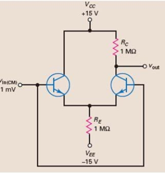
A) 15 mV
B) 1.5 mV
C) 0.5 mV
D) 0.5 V
A) 15 mV
B) 1.5 mV
C) 0.5 mV
D) 0.5 V
Question

Unlock Deck
Sign up to unlock the cards in this deck!
Unlock Deck
Unlock Deck
1/50
Play
Full screen (f)
Deck 15: Differential Amplifiers
1
The voltage gain of a differential amplifier divided by its common-mode voltage gain is referred to as the
A) input offset voltage.
B) common-mode rejection ratio.
C) differential output.
D) active load ratio.
A) input offset voltage.
B) common-mode rejection ratio.
C) differential output.
D) active load ratio.
B
2
Base resistors can produce input error voltages when the two halves of the diff amp are not perfectly symmetrical.
True
3
In order to get single-ended input operation using a diff amp,one of the inputs is used and the other input is grounded.
True
4
If compensation of an op amp becomes necessary,the best approach is to use
A) nulling circuits.
B) filtering circuits.
C) squelching circuits.
D) regulating circuits.
A) nulling circuits.
B) filtering circuits.
C) squelching circuits.
D) regulating circuits.
Unlock Deck
Unlock for access to all 50 flashcards in this deck.
Unlock Deck
k this deck
5
The input circuit used in most op amps is the common-collector amplifier.
Unlock Deck
Unlock for access to all 50 flashcards in this deck.
Unlock Deck
k this deck
6
A differential amplifier output requires that the load is single-ended and has one end grounded.
Unlock Deck
Unlock for access to all 50 flashcards in this deck.
Unlock Deck
k this deck
7
The input impedance of a diff amp is half as high as a single common-emitter amplifier.
Unlock Deck
Unlock for access to all 50 flashcards in this deck.
Unlock Deck
k this deck
8
When the noninverting and inverting input voltages of a differential amp are present,the output voltage equals the voltage gain times the difference of the two input voltages.
Unlock Deck
Unlock for access to all 50 flashcards in this deck.
Unlock Deck
k this deck
9
Components produced and connected during the manufacturing process on a small piece of semiconductor material are called
A) integrated circuits.
B) differential circuits.
C) CMOS.
D) discrete circuits.
A) integrated circuits.
B) differential circuits.
C) CMOS.
D) discrete circuits.
Unlock Deck
Unlock for access to all 50 flashcards in this deck.
Unlock Deck
k this deck
10
The term operational amplifier refers to an amplifier that performs a mathematical operation.
Unlock Deck
Unlock for access to all 50 flashcards in this deck.
Unlock Deck
k this deck
11
A diff amp is sometimes called a long-tail pair because the two transistors share a common collector resistor.
Unlock Deck
Unlock for access to all 50 flashcards in this deck.
Unlock Deck
k this deck
12
The input bias current of an op amp is defined as the sum of the dc base currents.
Unlock Deck
Unlock for access to all 50 flashcards in this deck.
Unlock Deck
k this deck
13
With diff amp configurations,when a single-ended output is used,the input may be noninverting or inverting.
Unlock Deck
Unlock for access to all 50 flashcards in this deck.
Unlock Deck
k this deck
14
The same input voltage that is applied to each base of a differential amplifier is called
A) complimentary signal.
B) nulling signal.
C) common-mode signal.
D) single-ended signal.
A) complimentary signal.
B) nulling signal.
C) common-mode signal.
D) single-ended signal.
Unlock Deck
Unlock for access to all 50 flashcards in this deck.
Unlock Deck
k this deck
15
The input offset voltage is defined as the input voltage that would produce the same output error voltage in a perfect diff amp.
Unlock Deck
Unlock for access to all 50 flashcards in this deck.
Unlock Deck
k this deck
16
The typical op amp is a dc amplifier with very high gain,very high input impedance,and very low output impedance.
Unlock Deck
Unlock for access to all 50 flashcards in this deck.
Unlock Deck
k this deck
17
The diff amp is extremely useful as the input stage of an op amp because
A) it has low input impedance.
B) it has a single-ended input.
C) it amplifies the common-mode signal.
D) it attenuates the common-mode signal.
A) it has low input impedance.
B) it has a single-ended input.
C) it amplifies the common-mode signal.
D) it attenuates the common-mode signal.
Unlock Deck
Unlock for access to all 50 flashcards in this deck.
Unlock Deck
k this deck
18
The three op amp data sheet characteristics that designers use when accurate answers are required are input bias current,input offset current,and input offset voltage.
Unlock Deck
Unlock for access to all 50 flashcards in this deck.
Unlock Deck
k this deck
19
With diff amp configurations,the voltage gain is maximum when a single-ended output is used.
Unlock Deck
Unlock for access to all 50 flashcards in this deck.
Unlock Deck
k this deck
20
The input offset current is defined as the difference of the dc base currents.
Unlock Deck
Unlock for access to all 50 flashcards in this deck.
Unlock Deck
k this deck
21
What can produce input error voltages when the two halves of the diff amp are not perfectly symmetrical?
A) collector resistors
B) emitter resistors
C) base resistors
D) coupling capacitors
A) collector resistors
B) emitter resistors
C) base resistors
D) coupling capacitors
Unlock Deck
Unlock for access to all 50 flashcards in this deck.
Unlock Deck
k this deck
22
In an op amp,the difference of the dc currents is called the
A) input offset current.
B) input bias current.
C) difference current.
D) dc mean current.
A) input offset current.
B) input bias current.
C) difference current.
D) dc mean current.
Unlock Deck
Unlock for access to all 50 flashcards in this deck.
Unlock Deck
k this deck
23
Data sheet characteristics that designers use for accurate answers do not include
A) input bias current.
B) input offset current.
C) input offset resistance.
D) input offset voltage.
A) input bias current.
B) input offset current.
C) input offset resistance.
D) input offset voltage.
Unlock Deck
Unlock for access to all 50 flashcards in this deck.
Unlock Deck
k this deck
24
The + symbol when used with an input of an op amp represents
A) the inverting input.
B) the noninverting input.
C) the differential input.
D) the single-ended input.
A) the inverting input.
B) the noninverting input.
C) the differential input.
D) the single-ended input.
Unlock Deck
Unlock for access to all 50 flashcards in this deck.
Unlock Deck
k this deck
25
Which of the following is not a characteristic of an op amp?
A) unity voltage gain
B) very high input impedance
C) very high voltage gain
D) very low output impedance
A) unity voltage gain
B) very high input impedance
C) very high voltage gain
D) very low output impedance
Unlock Deck
Unlock for access to all 50 flashcards in this deck.
Unlock Deck
k this deck
26
When both the noninverting and inverting input voltages are present,the total input is called a
A) single-ended input.
B) noninverting input.
C) differential input.
D) complimentary input.
A) single-ended input.
B) noninverting input.
C) differential input.
D) complimentary input.
Unlock Deck
Unlock for access to all 50 flashcards in this deck.
Unlock Deck
k this deck
27
The input impedance of a diff amp is
A) half as high as a single common-emitter stage.
B) twice as high as a single common-emitter stage.
C) the same as a single common-emitter stage.
D) four times as high as a single common-emitter stage.
A) half as high as a single common-emitter stage.
B) twice as high as a single common-emitter stage.
C) the same as a single common-emitter stage.
D) four times as high as a single common-emitter stage.
Unlock Deck
Unlock for access to all 50 flashcards in this deck.
Unlock Deck
k this deck
28
In order to get single-ended operation when using a diff amp
A) one input is used and the other is grounded.
B) one input is connected to the power supply and the other is grounded.
C) both inputs are used.
D) both inputs are grounded.
A) one input is used and the other is grounded.
B) one input is connected to the power supply and the other is grounded.
C) both inputs are used.
D) both inputs are grounded.
Unlock Deck
Unlock for access to all 50 flashcards in this deck.
Unlock Deck
k this deck
29
The input circuit used in most op amps is the
A) preamp.
B) tuned RF amp.
C) common-collector.
D) differential amp.
A) preamp.
B) tuned RF amp.
C) common-collector.
D) differential amp.
Unlock Deck
Unlock for access to all 50 flashcards in this deck.
Unlock Deck
k this deck
30
Because a diff amp shares a common emitter resistor,it is sometimes called
A) a sharing amp.
B) an emitter sharing amp.
C) a short-tail pair.
D) a long-tail pair.
A) a sharing amp.
B) an emitter sharing amp.
C) a short-tail pair.
D) a long-tail pair.
Unlock Deck
Unlock for access to all 50 flashcards in this deck.
Unlock Deck
k this deck
31
What are typically used as current sources and active loads in the design of IC op amps?
A) current limiters
B) zener regulators
C) current mirrors
D) current amps
A) current limiters
B) zener regulators
C) current mirrors
D) current amps
Unlock Deck
Unlock for access to all 50 flashcards in this deck.
Unlock Deck
k this deck
32
The most popular integrated circuits and the ICs manufactured with all components being part of one chip are called ________.
A) trivalent
B) pentavalent
C) duolithic
D) monolithic
A) trivalent
B) pentavalent
C) duolithic
D) monolithic
Unlock Deck
Unlock for access to all 50 flashcards in this deck.
Unlock Deck
k this deck
33
When two or more monolithic ICs are fabricated in one package,they are referred to as ________.
A) hybrid
B) thoroughbred
C) discrete
D) compensated
A) hybrid
B) thoroughbred
C) discrete
D) compensated
Unlock Deck
Unlock for access to all 50 flashcards in this deck.
Unlock Deck
k this deck
34
When a single-ended output of a differential amplifier is used,the input is
A) inverting only.
B) noninverting only.
C) differential only.
D) either inverting or noninverting.
A) inverting only.
B) noninverting only.
C) differential only.
D) either inverting or noninverting.
Unlock Deck
Unlock for access to all 50 flashcards in this deck.
Unlock Deck
k this deck
35
Components that are easily fabricated on a chip do not include ________.
A) transistors
B) capacitors
C) diodes
D) resistors
A) transistors
B) capacitors
C) diodes
D) resistors
Unlock Deck
Unlock for access to all 50 flashcards in this deck.
Unlock Deck
k this deck
36
Which diff amp configuration produces the maximum voltage gain?
A) differential input with differential output
B) differential input with single-ended output
C) single-ended input with differential output
D) single-ended input with single-ended output
A) differential input with differential output
B) differential input with single-ended output
C) single-ended input with differential output
D) single-ended input with single-ended output
Unlock Deck
Unlock for access to all 50 flashcards in this deck.
Unlock Deck
k this deck
37
In the manufacturing process of an IC,the procedure of sealing off the epitaxial layer with silicon dioxide is called ________,
A) compensation
B) sealation
C) passivation
D) crystallization
A) compensation
B) sealation
C) passivation
D) crystallization
Unlock Deck
Unlock for access to all 50 flashcards in this deck.
Unlock Deck
k this deck
38
In an op amp,the average of the dc base currents is referred to as
A) input offset current.
B) input bias current.
C) input average current.
D) base average current.
A) input offset current.
B) input bias current.
C) input average current.
D) base average current.
Unlock Deck
Unlock for access to all 50 flashcards in this deck.
Unlock Deck
k this deck
39
An amplifier that performs a mathematical operation is referred to as
A) a math amp.
B) an op amp.
C) a calc amp.
D) a comp amp.
A) a math amp.
B) an op amp.
C) a calc amp.
D) a comp amp.
Unlock Deck
Unlock for access to all 50 flashcards in this deck.
Unlock Deck
k this deck
40
The Intel P4 Prescott version microprocessor contains approximately
A) 125 transistors.
B) 125 thousand transistors.
C) 125 million transistors.
D) 125 billion transistors.
A) 125 transistors.
B) 125 thousand transistors.
C) 125 million transistors.
D) 125 billion transistors.
Unlock Deck
Unlock for access to all 50 flashcards in this deck.
Unlock Deck
k this deck
41
When a diff amp is amplifying the wanted signal and discriminating against the common-mode signal the CMRR is
A) high.
B) low.
C) less than 1.
D) equal to the common-mode voltage gain divided by the voltage gain.
A) high.
B) low.
C) less than 1.
D) equal to the common-mode voltage gain divided by the voltage gain.
Unlock Deck
Unlock for access to all 50 flashcards in this deck.
Unlock Deck
k this deck
42
Integrated circuits with fewer than 12 integrated components are referred to as
A) small-scale integration.
B) medium-scale integration.
C) large-scale integration.
D) very large scale integration.
A) small-scale integration.
B) medium-scale integration.
C) large-scale integration.
D) very large scale integration.
Unlock Deck
Unlock for access to all 50 flashcards in this deck.
Unlock Deck
k this deck
43
Ultra large scale integration refers to placing approximately how many components on a single chip?
A) 12 to 100
B) more than 100
C) thousands
D) more than a million
A) 12 to 100
B) more than 100
C) thousands
D) more than a million
Unlock Deck
Unlock for access to all 50 flashcards in this deck.
Unlock Deck
k this deck
44
When a differential amplifier is not perfectly symmetrical
A) there will be a small ac output voltage.
B) there will be no common-mode amplification.
C) there will be no ac output voltage.
D) there will be 0 V at the output.
A) there will be a small ac output voltage.
B) there will be no common-mode amplification.
C) there will be no ac output voltage.
D) there will be 0 V at the output.
Unlock Deck
Unlock for access to all 50 flashcards in this deck.
Unlock Deck
k this deck
45
Data sheets generally specify common-mode rejection ratio in ________.
A) mhos
B) volts
C) decibels
D) joules
A) mhos
B) volts
C) decibels
D) joules
Unlock Deck
Unlock for access to all 50 flashcards in this deck.
Unlock Deck
k this deck
46
What is the common-mode voltage gain for the circuit shown in Figure 15-21?
A) 1
B) 0.5
C) 1.5
D) 2
A) 1
B) 0.5
C) 1.5
D) 2
Unlock Deck
Unlock for access to all 50 flashcards in this deck.
Unlock Deck
k this deck
47
What op amp data sheet characteristic is defined as the input voltage that would produce the same output error voltage in a perfect diff amp?
A) input difference voltage
B) input error voltage
C) input bias voltage
D) input offset voltage
A) input difference voltage
B) input error voltage
C) input bias voltage
D) input offset voltage
Unlock Deck
Unlock for access to all 50 flashcards in this deck.
Unlock Deck
k this deck
48
What is the type of IC that is manufactured with resistors and capacitors integrated,but transistors and diodes are connected as discrete components?
A) thin film or thick film
B) analog
C) digital
D) hybrid
A) thin film or thick film
B) analog
C) digital
D) hybrid
Unlock Deck
Unlock for access to all 50 flashcards in this deck.
Unlock Deck
k this deck
49
What is the output voltage for the circuit shown in Figure 15-21?
A) 15 mV
B) 1.5 mV
C) 0.5 mV
D) 0.5 V
A) 15 mV
B) 1.5 mV
C) 0.5 mV
D) 0.5 V
Unlock Deck
Unlock for access to all 50 flashcards in this deck.
Unlock Deck
k this deck
50
The formula used to convert the CMRR to decibels is
A) 10 log CMRR.
B) 20 log CMRR.
C) 30 log CMRR.
D) 40 log CMRR.
A) 10 log CMRR.
B) 20 log CMRR.
C) 30 log CMRR.
D) 40 log CMRR.
Unlock Deck
Unlock for access to all 50 flashcards in this deck.
Unlock Deck
k this deck
Unlock Deck
Unlock for access to all 50 flashcards in this deck.


