Deck 2: Bipolar Junction Transistors BJTS
Full screen (f)
Question
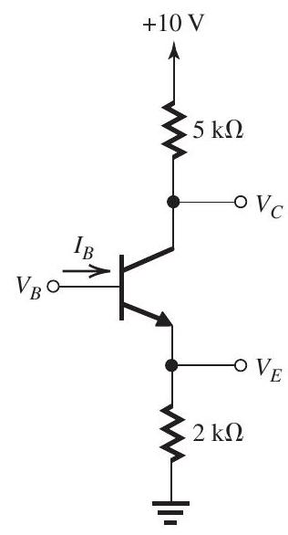
Figure 6.1.1
The BJT in the circuit in Fig. 6.1.1 has . Find , and for the three cases:
(a) , (b) , and (c) .
Question
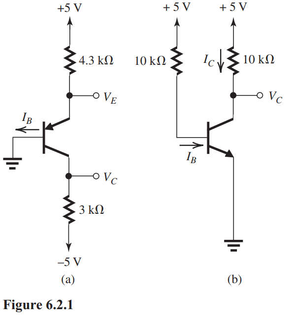
(a)The BJTs in the circuits of Fig. 6.2.1 have . (a) For the circuit in Fig. 6.2.1(a), find , and .
(b) For the circuit in Fig. 6.2.1(b), find , and .
Question
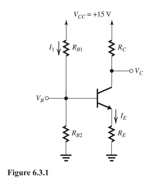
The transistor in the circuit of Fig. 6.3.1 has 100. Find the values of the four resistors so that , and .
Question
Figure 6.4.1
The BJTs in the circuit of Fig. 6.4.1 have and . Find for each of the following cases:
(a)
(b)
(c)
(d)
(e)
Question
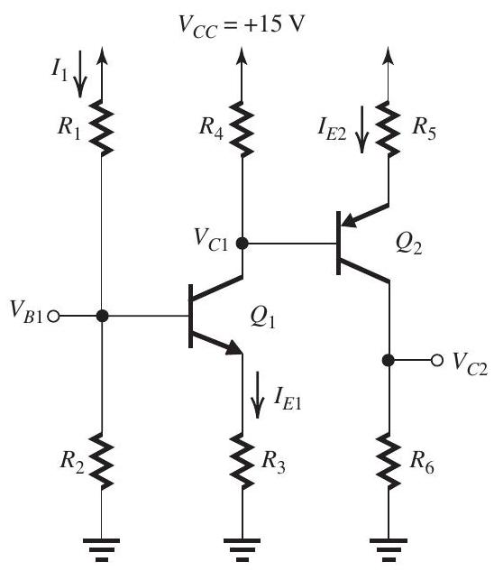
Figure 6.5.1
Design the circuit in Fig. 6.5.1 to obtain , , and . Let and . Specify the required values of all resistors.
Question
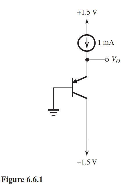
The BJT in the circuit in Fig. 6.6.1 has at room temperature.
(a) Find at room temperature where is .
(b) If the temperature increases by , what will become?
(c) If, alternatively, the temperature decreases by , what will become?

Unlock Deck
Sign up to unlock the cards in this deck!
Unlock Deck
Unlock Deck
1/6
Play
Full screen (f)
Deck 2: Bipolar Junction Transistors BJTS
1
Figure 6.1.1
The BJT in the circuit in Fig. 6.1.1 has . Find , and for the three cases:
(a) , (b) , and (c) .
(a)
Figure 6.1.2(a)
The solution is illustrated in Fig. 6.1.2(a). The transistor is cut off with
(b)
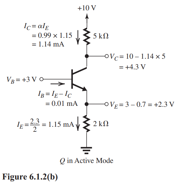
The solution is illustrated in Fig. 6.1.2(b). The transistor is operating in the active region with the following results:
(c)
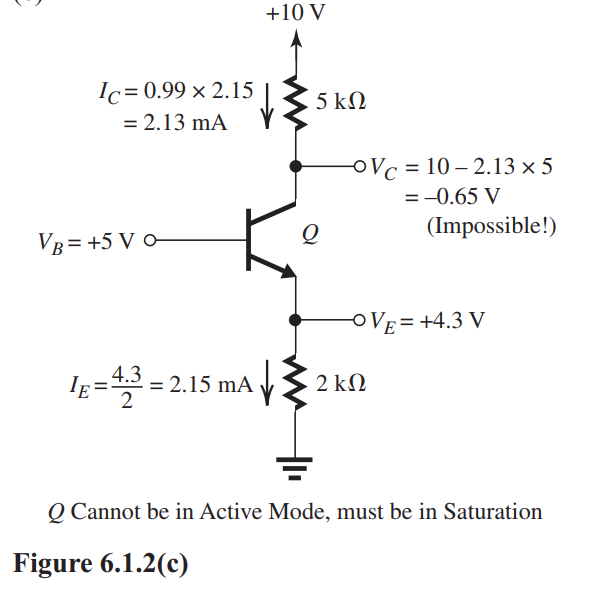
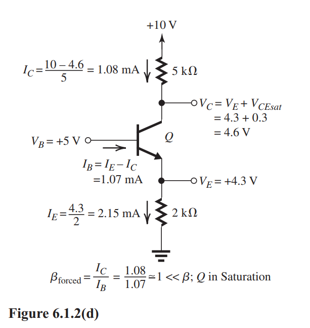
The analysis performed in Fig. 6.1.2(c) shows that the transistor cannot be operating in the active region. Thus, it must be saturated. The corresponding analysis is shown in Fig. 6.1.2(d) with the following results:
Figure 6.1.2(a)
The solution is illustrated in Fig. 6.1.2(a). The transistor is cut off with
(b)
The solution is illustrated in Fig. 6.1.2(b). The transistor is operating in the active region with the following results:
(c)
The analysis performed in Fig. 6.1.2(c) shows that the transistor cannot be operating in the active region. Thus, it must be saturated. The corresponding analysis is shown in Fig. 6.1.2(d) with the following results:
2
(a)The BJTs in the circuits of Fig. 6.2.1 have . (a) For the circuit in Fig. 6.2.1(a), find , and .
(b) For the circuit in Fig. 6.2.1(b), find , and .
(a)
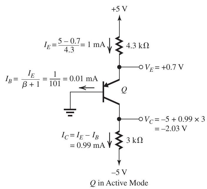
Figure 6.2.2(a)
The analysis is illustrated in Fig. 6.2.2(a). We have assumed that is operating in the active mode, and the results obtained justify this assumption: is lower than , keeping the CBJ reverse biased. The results are
(b)
cannot be in Active Mode; must be in Saturation
Figure 6.2.2(b)
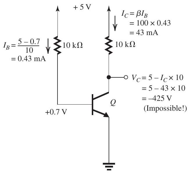
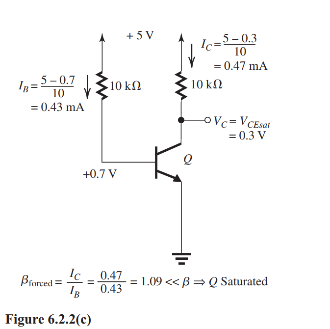 The analysis in Fig. 6.2.2(b) is based on the assumption that the transistor is operating in the active mode. The results obtained show that this assumption is not justified: at implies that the CBJ has a forward bias of ! Thus, the transistor must be in saturation. The corresponding analysis is shown in Fig. 6.2.2(c) and the results are
Figure 6.2.2(a)
The analysis is illustrated in Fig. 6.2.2(a). We have assumed that is operating in the active mode, and the results obtained justify this assumption: is lower than , keeping the CBJ reverse biased. The results are
(b)
cannot be in Active Mode; must be in Saturation
Figure 6.2.2(b)
The analysis in Fig. 6.2.2(b) is based on the assumption that the transistor is operating in the active mode. The results obtained show that this assumption is not justified: at implies that the CBJ has a forward bias of ! Thus, the transistor must be in saturation. The corresponding analysis is shown in Fig. 6.2.2(c) and the results are 3
The transistor in the circuit of Fig. 6.3.1 has 100. Find the values of the four resistors so that , and .
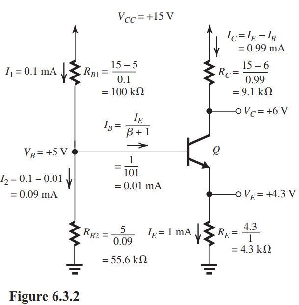
The complete solution is performed directly on the circuit diagram in Fig. 6.3.2. The solution is based on the fact that the transistor is operating in the active mode because . The results are
4
Figure 6.4.1
The BJTs in the circuit of Fig. 6.4.1 have and . Find for each of the following cases:
(a)
(b)
(c)
(d)
(e)
Unlock Deck
Unlock for access to all 6 flashcards in this deck.
Unlock Deck
k this deck
5
Figure 6.5.1
Design the circuit in Fig. 6.5.1 to obtain , , and . Let and . Specify the required values of all resistors.
Unlock Deck
Unlock for access to all 6 flashcards in this deck.
Unlock Deck
k this deck
6
The BJT in the circuit in Fig. 6.6.1 has at room temperature.
(a) Find at room temperature where is .
(b) If the temperature increases by , what will become?
(c) If, alternatively, the temperature decreases by , what will become?
Unlock Deck
Unlock for access to all 6 flashcards in this deck.
Unlock Deck
k this deck
Unlock Deck
Unlock for access to all 6 flashcards in this deck.


