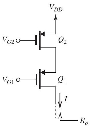
Solved

Figure 841
the Cascode Current Source in Fig μm\mu \mathrm{m} CMOS Process for Which

Question 2

Essay

     Figure 8.4.1 The cascode current source in Fig. 8.4.1 utilizes two identical PMOS transistors fabricated in a 0.18 -  \mu \mathrm{m}  CMOS process for which  V_{D D}=1.8 \mathrm{~V} ,  V_{t p}=-0.5 \mathrm{~V}, V_{A}^{\prime}=-6 \mathrm{~V} / \mu \mathrm{m} , and  \mu_{p} C_{o x}=   100 \mu \mathrm{A} / \mathrm{V}^{2} . Design the circuit to obtain  I=50 \mu \mathrm{A}  and  R_{O}=1 \mathrm{M} \Omega  and to allow for the maximum possible voltage swing at the output terminal of the current source. Utilize  \left|V_{O V}\right|=0.2 \mathrm{~V} . Specify the values of  L  and  W / L  for  Q_{1}  and  Q_{2} . As well, specify the required values of the dc bias voltages  V_{G 1}  and  V_{G 2} . What is the maximum allowable voltage at the output?

Figure 8.4.1
The cascode current source in Fig. 8.4.1 utilizes two identical PMOS transistors fabricated in a 0.18 - μm\mu \mathrm{m} CMOS process for which VDD=1.8 VV_{D D}=1.8 \mathrm{~V} , Vtp=0.5 V,VA=6 V/μmV_{t p}=-0.5 \mathrm{~V}, V_{A}^{\prime}=-6 \mathrm{~V} / \mu \mathrm{m} , and μpCox=\mu_{p} C_{o x}= 100μA/V2100 \mu \mathrm{A} / \mathrm{V}^{2} .
Design the circuit to obtain I=50μAI=50 \mu \mathrm{A} and RO=1MΩR_{O}=1 \mathrm{M} \Omega and to allow for the maximum possible voltage swing at the output terminal of the current source. Utilize VOV=0.2 V\left|V_{O V}\right|=0.2 \mathrm{~V} . Specify the values of LL and W/LW / L for Q1Q_{1} and Q2Q_{2} . As well, specify the required values of the dc bias voltages VG1V_{G 1} and VG2V_{G 2} . What is the maximum allowable voltage at the output?

Correct Answer:

verifed

Verified

Related Questions