Multiple Choice
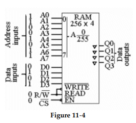
-What is the significance of the inverted triangles on the outputs of the device in Figure 11- 4?
A) They represent buffers and mean that the outputs can drive 40 TTL loads, instead of the normal 10.
B) It means that the outputs will only be active if a change has occurred at that memory location since the last read/write cycle.
C) They represent inverters and mean that the outputs are active- LOW.
D) The IC has tri- state outputs.
Correct Answer:

Verified
Correct Answer:
Verified
Q2: The checksum method is used to test
Q3: ROM access time is defined as _.<br>A)
Q4: <img src="https://d2lvgg3v3hfg70.cloudfront.net/TB9838/.jpg" alt=" -The block identified
Q5: DIMMS generally contain DDR SDRAM memory chips.
Q6: <img src="https://d2lvgg3v3hfg70.cloudfront.net/TB9838/.jpg" alt=" -What memory location
Q7: Fusible link PROMs are programmed removing the
Q8: RAMs must have a ? <img src="https://d2lvgg3v3hfg70.cloudfront.net/TB9838/.jpg"
Q9: A FIFO _.<br>A) allows data to be
Q10: <img src="https://d2lvgg3v3hfg70.cloudfront.net/TB9838/.jpg" alt=" -What are the
Q11: A DIMM _.<br>A) has contact pins on