Essay
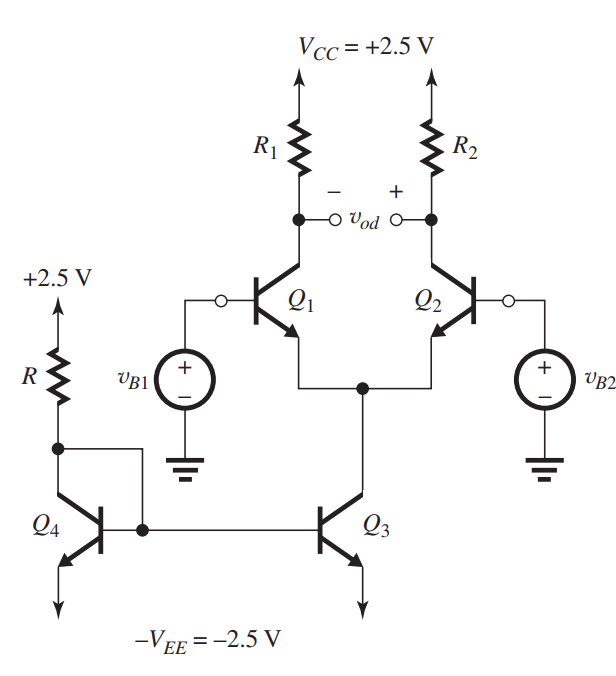
Figure 9.4.1
For the circuit shown in Fig. 9.4.1, neglect base currents in dc calculations and assume that for each transistor . Transistors and are perfectly matched. Transistor has twice the emitter-base junction area of .
(a) For , design the circuit to establish a dc bias current of in the collector of each of and and a dc voltage of at the collector of each of and . Specify the values required for , and .
(b) For and , determine the differential small-signal voltage gain . Ignore the Early effect. If , what is the differential input resistance of the differential amplifier ?
(c) If has an Early voltage of , find its output resistance and use this result to determine the common-mode gain of the differential amplifier , where and assuming that each of and is accurate to within . What is the resulting CMRR in decibels?
Correct Answer:

Verified
Correct Answer:
Verified
Q2: <img src="https://d2lvgg3v3hfg70.cloudfront.net/TBO1243/.jpg" alt="
Q3: Refer to Figure 9.10.1 below. <br>
Q4: <img src="https://d2lvgg3v3hfg70.cloudfront.net/TBO1243/.jpg" alt="
Q5: <img src="https://d2lvgg3v3hfg70.cloudfront.net/TBO1243/.jpg" alt="
Q6: <img src="https://d2lvgg3v3hfg70.cloudfront.net/TBO1243/.jpg" alt="
Q7: <img src="https://d2lvgg3v3hfg70.cloudfront.net/TBO1243/.jpg" alt="
Q8: <img src="https://d2lvgg3v3hfg70.cloudfront.net/TBO1243/.jpg" alt="
Q9: <img src="https://d2lvgg3v3hfg70.cloudfront.net/TBO1243/.jpg" alt="
Q10: <img src="https://d2lvgg3v3hfg70.cloudfront.net/TBO1243/.jpg" alt="