Exam 1: MOS Field-Effect Transistors Mosfets
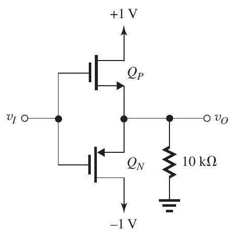 Figure 5.6.1
The transistors in the circuit of Fig. 5.6.1 have and . Find for each of the following cases:
(a)
(b)
(c)
(d)
(e)
Figure 5.6.1
The transistors in the circuit of Fig. 5.6.1 have and . Find for each of the following cases:
(a)
(b)
(c)
(d)
(e)
(a)
![(a) Figure 5.6.2 From Fig. 5.6.2, we see that when v_{I}=0 \mathrm{~V} , both transistors are cut off and v_{O}=0 \mathrm{~V} (b) With v_{I}=+1 \mathrm{~V}, Q_{P} cannot conduct and can be eliminated, reducing the circuit to that shown in Fig. 5.6.3. Since v_{G D N}=0 \mathrm{~V}, Q_{N} will be operating in saturation with i_{D}=\frac{1}{2} k_{n}\left(v_{G S}-V_{t n}\right)^{2} But i_{D}=\frac{v_{O}}{10 \mathrm{k} \Omega}=0.1 v_{O}, \quad \mathrm{~mA} and v_{G S}=v_{I}-v_{O}=1-v_{O} Thus, \begin{aligned} 0.1 v_{O} & =\frac{1}{2} \times 2\left(1-v_{O}-0.4\right)^{2} \\ & =\left(0.6-v_{O}\right)^{2} \\ & =0.36-1.2 v_{O}+v_{O}^{2} \end{aligned} which can be rearranged in the form v_{O}^{2}-1.3 v_{O}+0.36=0 This quadratic has two solutions: 0.775 \mathrm{~V} , which is physically meaningless since v_{G S} becomes 1- 0.775=0.225 \mathrm{~V} , which is less than V_{t n} ; and 0.4 \mathrm{~V} , which is possible. Thus, v_{O}=0.4 \mathrm{~V} (c) Figure 5.6.4 With v_{I}=-1 \mathrm{~V}, Q_{N} cannot conduct and can be eliminated, reducing the circuit to that shown in Fig. 5.6.4. Since v_{G D P}=0 \mathrm{~V}, Q_{P} will be operating in saturation. We recognize this situation to be the complement of that in (b) above. Thus, we do not need to do the analysis again and we can simply write v_{O}=-0.4 \mathrm{~V} (d) With v_{I}=+2 \mathrm{~V}, Q_{P} cannot conduct and can be removed, thus reducing the circuit to that shown in Fig. 5.6.5. Since v_{G D N}=1 \mathrm{~V} , which is greater than V_{t n}, Q_{N} will be operating in the triode region. Thus, i_{D}=k_{n}\left[\left(v_{G S}-V_{t n}\right) v_{D S}-\frac{1}{2} v_{D S}^{2}\right] Here, \begin{aligned} i_{D} & =\frac{v_{O}}{10 \mathrm{k} \Omega}=0.1 v_{O}, \quad \mathrm{~mA} \\ v_{G S} & =2-v_{O} \\ v_{D S} & =1-v_{O} \end{aligned} Thus, \begin{aligned} 0.1 v_{O} & =2\left[\left(1.6-v_{O}\right)\left(1-v_{O}\right)-\frac{1}{2}\left(1-v_{O}\right)^{2}\right] \\ & =2\left[1.6-2.6 v_{O}+v_{O}^{2}-\frac{1}{2}+v_{O}-\frac{1}{2} v_{O}^{2}\right] \\ & =v_{O}^{2}-3.2 v_{O}+2.2 \\ & \Rightarrow v_{O}^{2}-3.3 v_{O}+2.2=0 \end{aligned} which has the following solution v_{O}=\frac{+3.3 \pm \sqrt{3.3^{2}-8.8}}{2}=0.927 \mathrm{~V} \text { or } 2.37 \mathrm{~V} The second solution is physically meaningless as v_{O} exceeds v_{D} . Thus, v_{O}=0.927 \mathrm{~V} (e) Figure 5.6.6 With v_{I}=-2 \mathrm{~V}, Q_{N} cannot conduct and the circuit reduces to that shown in Fig. 5.6.6. We recognize this situation to be the complement of that in (d) above. Thus, v_{O}=-0.927 \mathrm{~V}](https://storage.examlex.com/TBO1243/11eeb9e9_cbc9_7579_9342_b129b2eb58cc_TBO1243_00.jpg)
Figure 5.6.2
From Fig. 5.6.2, we see that when , both transistors are cut off and
(b)
![(a) Figure 5.6.2 From Fig. 5.6.2, we see that when v_{I}=0 \mathrm{~V} , both transistors are cut off and v_{O}=0 \mathrm{~V} (b) With v_{I}=+1 \mathrm{~V}, Q_{P} cannot conduct and can be eliminated, reducing the circuit to that shown in Fig. 5.6.3. Since v_{G D N}=0 \mathrm{~V}, Q_{N} will be operating in saturation with i_{D}=\frac{1}{2} k_{n}\left(v_{G S}-V_{t n}\right)^{2} But i_{D}=\frac{v_{O}}{10 \mathrm{k} \Omega}=0.1 v_{O}, \quad \mathrm{~mA} and v_{G S}=v_{I}-v_{O}=1-v_{O} Thus, \begin{aligned} 0.1 v_{O} & =\frac{1}{2} \times 2\left(1-v_{O}-0.4\right)^{2} \\ & =\left(0.6-v_{O}\right)^{2} \\ & =0.36-1.2 v_{O}+v_{O}^{2} \end{aligned} which can be rearranged in the form v_{O}^{2}-1.3 v_{O}+0.36=0 This quadratic has two solutions: 0.775 \mathrm{~V} , which is physically meaningless since v_{G S} becomes 1- 0.775=0.225 \mathrm{~V} , which is less than V_{t n} ; and 0.4 \mathrm{~V} , which is possible. Thus, v_{O}=0.4 \mathrm{~V} (c) Figure 5.6.4 With v_{I}=-1 \mathrm{~V}, Q_{N} cannot conduct and can be eliminated, reducing the circuit to that shown in Fig. 5.6.4. Since v_{G D P}=0 \mathrm{~V}, Q_{P} will be operating in saturation. We recognize this situation to be the complement of that in (b) above. Thus, we do not need to do the analysis again and we can simply write v_{O}=-0.4 \mathrm{~V} (d) With v_{I}=+2 \mathrm{~V}, Q_{P} cannot conduct and can be removed, thus reducing the circuit to that shown in Fig. 5.6.5. Since v_{G D N}=1 \mathrm{~V} , which is greater than V_{t n}, Q_{N} will be operating in the triode region. Thus, i_{D}=k_{n}\left[\left(v_{G S}-V_{t n}\right) v_{D S}-\frac{1}{2} v_{D S}^{2}\right] Here, \begin{aligned} i_{D} & =\frac{v_{O}}{10 \mathrm{k} \Omega}=0.1 v_{O}, \quad \mathrm{~mA} \\ v_{G S} & =2-v_{O} \\ v_{D S} & =1-v_{O} \end{aligned} Thus, \begin{aligned} 0.1 v_{O} & =2\left[\left(1.6-v_{O}\right)\left(1-v_{O}\right)-\frac{1}{2}\left(1-v_{O}\right)^{2}\right] \\ & =2\left[1.6-2.6 v_{O}+v_{O}^{2}-\frac{1}{2}+v_{O}-\frac{1}{2} v_{O}^{2}\right] \\ & =v_{O}^{2}-3.2 v_{O}+2.2 \\ & \Rightarrow v_{O}^{2}-3.3 v_{O}+2.2=0 \end{aligned} which has the following solution v_{O}=\frac{+3.3 \pm \sqrt{3.3^{2}-8.8}}{2}=0.927 \mathrm{~V} \text { or } 2.37 \mathrm{~V} The second solution is physically meaningless as v_{O} exceeds v_{D} . Thus, v_{O}=0.927 \mathrm{~V} (e) Figure 5.6.6 With v_{I}=-2 \mathrm{~V}, Q_{N} cannot conduct and the circuit reduces to that shown in Fig. 5.6.6. We recognize this situation to be the complement of that in (d) above. Thus, v_{O}=-0.927 \mathrm{~V}](https://storage.examlex.com/TBO1243/11eeb9e9_cbc9_757a_9342_8f3464082e64_TBO1243_00.jpg)
With cannot conduct and can be eliminated, reducing the circuit to that shown in Fig. 5.6.3. Since will be operating in saturation with
But
and
Thus,
which can be rearranged in the form
This quadratic has two solutions: , which is physically meaningless since becomes , which is less than ; and , which is possible. Thus,
(c)
![(a) Figure 5.6.2 From Fig. 5.6.2, we see that when v_{I}=0 \mathrm{~V} , both transistors are cut off and v_{O}=0 \mathrm{~V} (b) With v_{I}=+1 \mathrm{~V}, Q_{P} cannot conduct and can be eliminated, reducing the circuit to that shown in Fig. 5.6.3. Since v_{G D N}=0 \mathrm{~V}, Q_{N} will be operating in saturation with i_{D}=\frac{1}{2} k_{n}\left(v_{G S}-V_{t n}\right)^{2} But i_{D}=\frac{v_{O}}{10 \mathrm{k} \Omega}=0.1 v_{O}, \quad \mathrm{~mA} and v_{G S}=v_{I}-v_{O}=1-v_{O} Thus, \begin{aligned} 0.1 v_{O} & =\frac{1}{2} \times 2\left(1-v_{O}-0.4\right)^{2} \\ & =\left(0.6-v_{O}\right)^{2} \\ & =0.36-1.2 v_{O}+v_{O}^{2} \end{aligned} which can be rearranged in the form v_{O}^{2}-1.3 v_{O}+0.36=0 This quadratic has two solutions: 0.775 \mathrm{~V} , which is physically meaningless since v_{G S} becomes 1- 0.775=0.225 \mathrm{~V} , which is less than V_{t n} ; and 0.4 \mathrm{~V} , which is possible. Thus, v_{O}=0.4 \mathrm{~V} (c) Figure 5.6.4 With v_{I}=-1 \mathrm{~V}, Q_{N} cannot conduct and can be eliminated, reducing the circuit to that shown in Fig. 5.6.4. Since v_{G D P}=0 \mathrm{~V}, Q_{P} will be operating in saturation. We recognize this situation to be the complement of that in (b) above. Thus, we do not need to do the analysis again and we can simply write v_{O}=-0.4 \mathrm{~V} (d) With v_{I}=+2 \mathrm{~V}, Q_{P} cannot conduct and can be removed, thus reducing the circuit to that shown in Fig. 5.6.5. Since v_{G D N}=1 \mathrm{~V} , which is greater than V_{t n}, Q_{N} will be operating in the triode region. Thus, i_{D}=k_{n}\left[\left(v_{G S}-V_{t n}\right) v_{D S}-\frac{1}{2} v_{D S}^{2}\right] Here, \begin{aligned} i_{D} & =\frac{v_{O}}{10 \mathrm{k} \Omega}=0.1 v_{O}, \quad \mathrm{~mA} \\ v_{G S} & =2-v_{O} \\ v_{D S} & =1-v_{O} \end{aligned} Thus, \begin{aligned} 0.1 v_{O} & =2\left[\left(1.6-v_{O}\right)\left(1-v_{O}\right)-\frac{1}{2}\left(1-v_{O}\right)^{2}\right] \\ & =2\left[1.6-2.6 v_{O}+v_{O}^{2}-\frac{1}{2}+v_{O}-\frac{1}{2} v_{O}^{2}\right] \\ & =v_{O}^{2}-3.2 v_{O}+2.2 \\ & \Rightarrow v_{O}^{2}-3.3 v_{O}+2.2=0 \end{aligned} which has the following solution v_{O}=\frac{+3.3 \pm \sqrt{3.3^{2}-8.8}}{2}=0.927 \mathrm{~V} \text { or } 2.37 \mathrm{~V} The second solution is physically meaningless as v_{O} exceeds v_{D} . Thus, v_{O}=0.927 \mathrm{~V} (e) Figure 5.6.6 With v_{I}=-2 \mathrm{~V}, Q_{N} cannot conduct and the circuit reduces to that shown in Fig. 5.6.6. We recognize this situation to be the complement of that in (d) above. Thus, v_{O}=-0.927 \mathrm{~V}](https://storage.examlex.com/TBO1243/11eeb9e9_cbc9_757b_9342_853c0b0ce14b_TBO1243_00.jpg)
Figure 5.6.4
With cannot conduct and can be eliminated, reducing the circuit to that shown in Fig. 5.6.4. Since will be operating in saturation. We recognize this situation to be the complement of that in (b) above. Thus, we do not need to do the analysis again and we can simply write
(d)
![(a) Figure 5.6.2 From Fig. 5.6.2, we see that when v_{I}=0 \mathrm{~V} , both transistors are cut off and v_{O}=0 \mathrm{~V} (b) With v_{I}=+1 \mathrm{~V}, Q_{P} cannot conduct and can be eliminated, reducing the circuit to that shown in Fig. 5.6.3. Since v_{G D N}=0 \mathrm{~V}, Q_{N} will be operating in saturation with i_{D}=\frac{1}{2} k_{n}\left(v_{G S}-V_{t n}\right)^{2} But i_{D}=\frac{v_{O}}{10 \mathrm{k} \Omega}=0.1 v_{O}, \quad \mathrm{~mA} and v_{G S}=v_{I}-v_{O}=1-v_{O} Thus, \begin{aligned} 0.1 v_{O} & =\frac{1}{2} \times 2\left(1-v_{O}-0.4\right)^{2} \\ & =\left(0.6-v_{O}\right)^{2} \\ & =0.36-1.2 v_{O}+v_{O}^{2} \end{aligned} which can be rearranged in the form v_{O}^{2}-1.3 v_{O}+0.36=0 This quadratic has two solutions: 0.775 \mathrm{~V} , which is physically meaningless since v_{G S} becomes 1- 0.775=0.225 \mathrm{~V} , which is less than V_{t n} ; and 0.4 \mathrm{~V} , which is possible. Thus, v_{O}=0.4 \mathrm{~V} (c) Figure 5.6.4 With v_{I}=-1 \mathrm{~V}, Q_{N} cannot conduct and can be eliminated, reducing the circuit to that shown in Fig. 5.6.4. Since v_{G D P}=0 \mathrm{~V}, Q_{P} will be operating in saturation. We recognize this situation to be the complement of that in (b) above. Thus, we do not need to do the analysis again and we can simply write v_{O}=-0.4 \mathrm{~V} (d) With v_{I}=+2 \mathrm{~V}, Q_{P} cannot conduct and can be removed, thus reducing the circuit to that shown in Fig. 5.6.5. Since v_{G D N}=1 \mathrm{~V} , which is greater than V_{t n}, Q_{N} will be operating in the triode region. Thus, i_{D}=k_{n}\left[\left(v_{G S}-V_{t n}\right) v_{D S}-\frac{1}{2} v_{D S}^{2}\right] Here, \begin{aligned} i_{D} & =\frac{v_{O}}{10 \mathrm{k} \Omega}=0.1 v_{O}, \quad \mathrm{~mA} \\ v_{G S} & =2-v_{O} \\ v_{D S} & =1-v_{O} \end{aligned} Thus, \begin{aligned} 0.1 v_{O} & =2\left[\left(1.6-v_{O}\right)\left(1-v_{O}\right)-\frac{1}{2}\left(1-v_{O}\right)^{2}\right] \\ & =2\left[1.6-2.6 v_{O}+v_{O}^{2}-\frac{1}{2}+v_{O}-\frac{1}{2} v_{O}^{2}\right] \\ & =v_{O}^{2}-3.2 v_{O}+2.2 \\ & \Rightarrow v_{O}^{2}-3.3 v_{O}+2.2=0 \end{aligned} which has the following solution v_{O}=\frac{+3.3 \pm \sqrt{3.3^{2}-8.8}}{2}=0.927 \mathrm{~V} \text { or } 2.37 \mathrm{~V} The second solution is physically meaningless as v_{O} exceeds v_{D} . Thus, v_{O}=0.927 \mathrm{~V} (e) Figure 5.6.6 With v_{I}=-2 \mathrm{~V}, Q_{N} cannot conduct and the circuit reduces to that shown in Fig. 5.6.6. We recognize this situation to be the complement of that in (d) above. Thus, v_{O}=-0.927 \mathrm{~V}](https://storage.examlex.com/TBO1243/11eeb9e9_cbc9_757c_9342_8105896402f0_TBO1243_00.jpg)
With cannot conduct and can be removed, thus reducing the circuit to that shown in Fig. 5.6.5. Since , which is greater than will be operating in the triode region. Thus,
Here,
Thus,
which has the following solution
The second solution is physically meaningless as exceeds . Thus,
(e)
![(a) Figure 5.6.2 From Fig. 5.6.2, we see that when v_{I}=0 \mathrm{~V} , both transistors are cut off and v_{O}=0 \mathrm{~V} (b) With v_{I}=+1 \mathrm{~V}, Q_{P} cannot conduct and can be eliminated, reducing the circuit to that shown in Fig. 5.6.3. Since v_{G D N}=0 \mathrm{~V}, Q_{N} will be operating in saturation with i_{D}=\frac{1}{2} k_{n}\left(v_{G S}-V_{t n}\right)^{2} But i_{D}=\frac{v_{O}}{10 \mathrm{k} \Omega}=0.1 v_{O}, \quad \mathrm{~mA} and v_{G S}=v_{I}-v_{O}=1-v_{O} Thus, \begin{aligned} 0.1 v_{O} & =\frac{1}{2} \times 2\left(1-v_{O}-0.4\right)^{2} \\ & =\left(0.6-v_{O}\right)^{2} \\ & =0.36-1.2 v_{O}+v_{O}^{2} \end{aligned} which can be rearranged in the form v_{O}^{2}-1.3 v_{O}+0.36=0 This quadratic has two solutions: 0.775 \mathrm{~V} , which is physically meaningless since v_{G S} becomes 1- 0.775=0.225 \mathrm{~V} , which is less than V_{t n} ; and 0.4 \mathrm{~V} , which is possible. Thus, v_{O}=0.4 \mathrm{~V} (c) Figure 5.6.4 With v_{I}=-1 \mathrm{~V}, Q_{N} cannot conduct and can be eliminated, reducing the circuit to that shown in Fig. 5.6.4. Since v_{G D P}=0 \mathrm{~V}, Q_{P} will be operating in saturation. We recognize this situation to be the complement of that in (b) above. Thus, we do not need to do the analysis again and we can simply write v_{O}=-0.4 \mathrm{~V} (d) With v_{I}=+2 \mathrm{~V}, Q_{P} cannot conduct and can be removed, thus reducing the circuit to that shown in Fig. 5.6.5. Since v_{G D N}=1 \mathrm{~V} , which is greater than V_{t n}, Q_{N} will be operating in the triode region. Thus, i_{D}=k_{n}\left[\left(v_{G S}-V_{t n}\right) v_{D S}-\frac{1}{2} v_{D S}^{2}\right] Here, \begin{aligned} i_{D} & =\frac{v_{O}}{10 \mathrm{k} \Omega}=0.1 v_{O}, \quad \mathrm{~mA} \\ v_{G S} & =2-v_{O} \\ v_{D S} & =1-v_{O} \end{aligned} Thus, \begin{aligned} 0.1 v_{O} & =2\left[\left(1.6-v_{O}\right)\left(1-v_{O}\right)-\frac{1}{2}\left(1-v_{O}\right)^{2}\right] \\ & =2\left[1.6-2.6 v_{O}+v_{O}^{2}-\frac{1}{2}+v_{O}-\frac{1}{2} v_{O}^{2}\right] \\ & =v_{O}^{2}-3.2 v_{O}+2.2 \\ & \Rightarrow v_{O}^{2}-3.3 v_{O}+2.2=0 \end{aligned} which has the following solution v_{O}=\frac{+3.3 \pm \sqrt{3.3^{2}-8.8}}{2}=0.927 \mathrm{~V} \text { or } 2.37 \mathrm{~V} The second solution is physically meaningless as v_{O} exceeds v_{D} . Thus, v_{O}=0.927 \mathrm{~V} (e) Figure 5.6.6 With v_{I}=-2 \mathrm{~V}, Q_{N} cannot conduct and the circuit reduces to that shown in Fig. 5.6.6. We recognize this situation to be the complement of that in (d) above. Thus, v_{O}=-0.927 \mathrm{~V}](https://storage.examlex.com/TBO1243/11eeb9e9_cbc9_757d_9342_dd016f9d1f27_TBO1243_00.jpg)
Figure 5.6.6
With cannot conduct and the circuit reduces to that shown in Fig. 5.6.6. We recognize this situation to be the complement of that in (d) above. Thus,
![Figure 5.1.1 (a) For the circuit shown in Fig. 5.1.1(a), show (neglecting \lambda ) that V=V_{t}+\sqrt{\frac{2 I}{k_{n}^{\prime}(W / L)}} (b) The MOSFETs in the circuit of Fig. 5.1.1(b) [6 points] have V_{t}=0.4 \mathrm{~V}, k_{n}^{\prime}=0.4 \mathrm{~mA} / \mathrm{V}^{2} , and \lambda=0 . Find (W / L)_{1},(W / L)_{2} , and (W / L)_{3} to obtain the reference voltages shown.](https://storage.examlex.com/TBO1243/11eeb9e9_cbc8_b212_9342_ebf986ba8fec_TBO1243_00.jpg) Figure 5.1.1
(a) For the circuit shown in Fig. 5.1.1(a), show (neglecting ) that
(b) The MOSFETs in the circuit of Fig. 5.1.1(b) [6 points] have , and . Find , and to obtain the reference voltages shown.
Figure 5.1.1
(a) For the circuit shown in Fig. 5.1.1(a), show (neglecting ) that
(b) The MOSFETs in the circuit of Fig. 5.1.1(b) [6 points] have , and . Find , and to obtain the reference voltages shown.
(a)
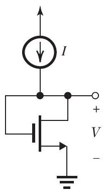
Figure 5.1.1(a)
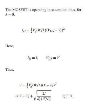
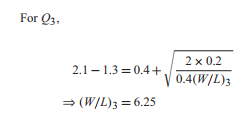
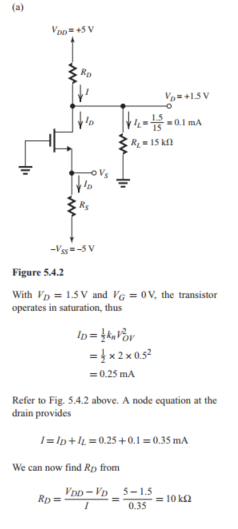
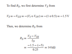
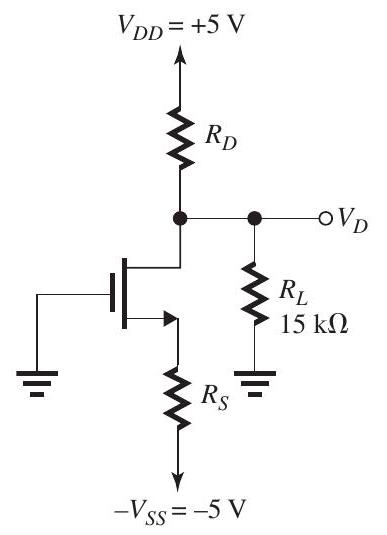 Figure 5.4.1
The MOSFET in the circuit of Fig. 5.4.1 has and , and the Early effect can be neglected.
(a) Find the values of and that result in the MOSFET operating with an overdrive voltage of and a drain voltage of . What is the resulting value?
(b) If is reduced from to , what does become?
(c) If is disconnected, what does become?
(d) With disconnected, what is the largest that can be used while the MOSFET is remaining in saturation?
Figure 5.4.1
The MOSFET in the circuit of Fig. 5.4.1 has and , and the Early effect can be neglected.
(a) Find the values of and that result in the MOSFET operating with an overdrive voltage of and a drain voltage of . What is the resulting value?
(b) If is reduced from to , what does become?
(c) If is disconnected, what does become?
(d) With disconnected, what is the largest that can be used while the MOSFET is remaining in saturation?
(b) Refer to Figure 5.4 .3 below.
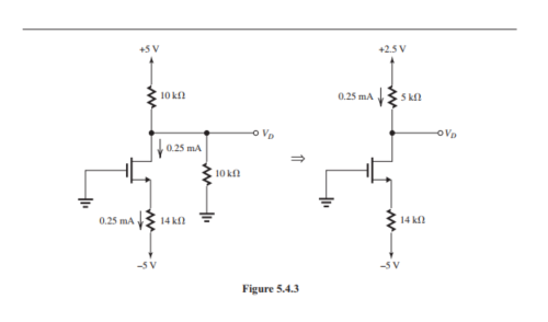
We assume that with reduced to , the MOSFET remains in saturation. Thus, remains unchanged at 0.25 . Figure 5.4.3 shows the circuit before and after Thévenin theorem is applied to simplify the drain circuit. Now,
Thus, , and saturation-mode operation is confirmed. The drain voltage becomes
(c)
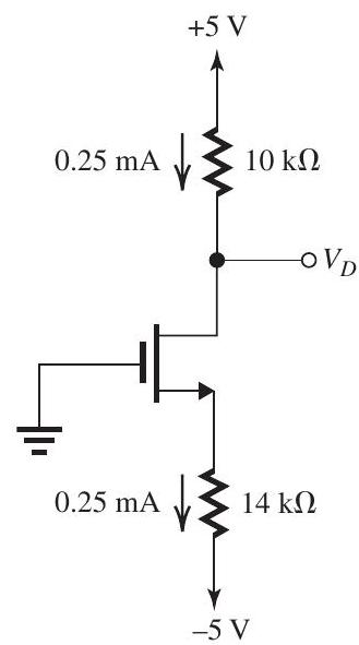
Figure 5.4.4
If is disconnected, the circuit becomes as in Fig. 5.4.4. Assuming that the transistor remains in saturation, then and
which is greater than , thus confirming saturation-mode operation. The drain voltage is now
(d)
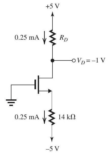
Figure 5.4.5
With disconnected and the MOSFET operating at the edge of saturation, , thus
and the current remains unchanged,
From the circuit in Fig. 5.4.5, we can write
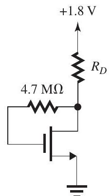
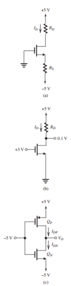 Figure 5.5.1
The MOSFETs in the circuits of Fig. 5.5.1 have , and .
(a) For the circuit in Fig. 5.5.1(a), find the values of and that result in the MOSFET operating at the edge of the saturation region with .
(b) For the circuit in Fig. 5.5.1(b), find and .
(c) For the circuit in Fig. 5.5.1(c), find , and . Also, find the drain-to-source incremental resistance of each of and .
Figure 5.5.1
The MOSFETs in the circuits of Fig. 5.5.1 have , and .
(a) For the circuit in Fig. 5.5.1(a), find the values of and that result in the MOSFET operating at the edge of the saturation region with .
(b) For the circuit in Fig. 5.5.1(b), find and .
(c) For the circuit in Fig. 5.5.1(c), find , and . Also, find the drain-to-source incremental resistance of each of and .
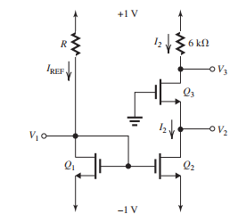 Figure 5.7.1
The MOSFETs in the circuit of Fig. 5.7.1 have , and . Find to obtain a reference current of . Also, find the values of , and .
Figure 5.7.1
The MOSFETs in the circuit of Fig. 5.7.1 have , and . Find to obtain a reference current of . Also, find the values of , and .
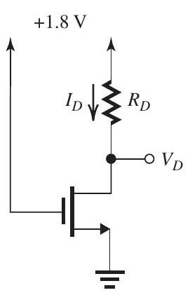 Figure 5.3.1
The MOSFET in Fig. 5.3.1 has , and . Find the value of that results in
i.
ii.
In each case, find and the incremental drain-tosource resistance of the MOSFET.
Figure 5.3.1
The MOSFET in Fig. 5.3.1 has , and . Find the value of that results in
i.
ii.
In each case, find and the incremental drain-tosource resistance of the MOSFET.
 (a)
(a)
 (b)
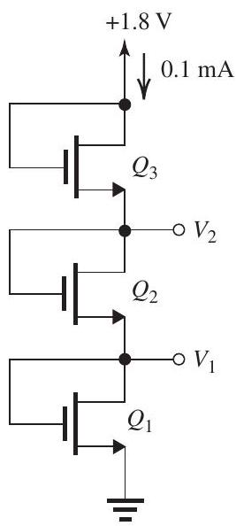
Figure 5.2.1
The MOSFETs in the circuits of Fig. 5.2.1 have , and .
(a) For the circuit in Fig. 5.2.1(a), find the values of and to operate the MOSFET at and .
(b) For the circuit in Fig. 5.2.1(b), find , and to obtain and .
(b)
Figure 5.2.1
The MOSFETs in the circuits of Fig. 5.2.1 have , and .
(a) For the circuit in Fig. 5.2.1(a), find the values of and to operate the MOSFET at and .
(b) For the circuit in Fig. 5.2.1(b), find , and to obtain and .
Filters
- Essay(0)
- Multiple Choice(0)
- Short Answer(0)
- True False(0)
- Matching(0)