Exam 4: Building Blocks of Integrated-Circuit Amplifiers
Exam 1: MOS Field-Effect Transistors Mosfets7 Questions
Exam 2: Bipolar Junction Transistors BJTS6 Questions
Exam 3: Transistor Amplifiers8 Questions
Exam 4: Building Blocks of Integrated-Circuit Amplifiers5 Questions
Exam 5: Differential and Multistage Amplifiers10 Questions
Exam 6: Frequency Response10 Questions
Exam 7: Feedback9 Questions
Exam 8: Operational Amplifier Circuits, Filters, Oscillators and CMOS Digital Logic Circuits9 Questions
Select questions type
Given the availability of NMOS and PMOS transistors that are matched and have and , give circuits for the following amplifiers. In each case, find the output resistance and the voltage gain. In all cases, operate each transistor at a dc bias current of and give the value of at which each transistor is operating.
(a) An NMOS common-source amplifier with a PMOS current-source load.
(b) An NMOS common-source amplifier with an NMOS cascode stage and a single-transistor PMOS current-source load.
(c) An NMOS common-source amplifier with an NMOS cascode stage and a cascode PMOS current-source load.
Free
(Essay)
4.9/5  (42)
(42)
Correct Answer: Verified
For each transistor,
(a)
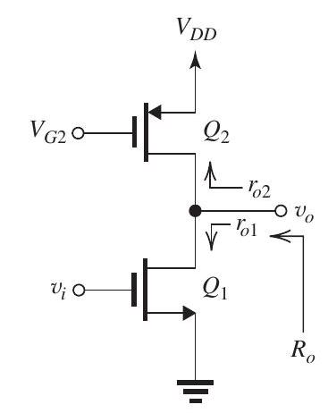
Figure 8.2.1
See Figure 8.2.1.
(b)
Figure 8.2.2
(c)
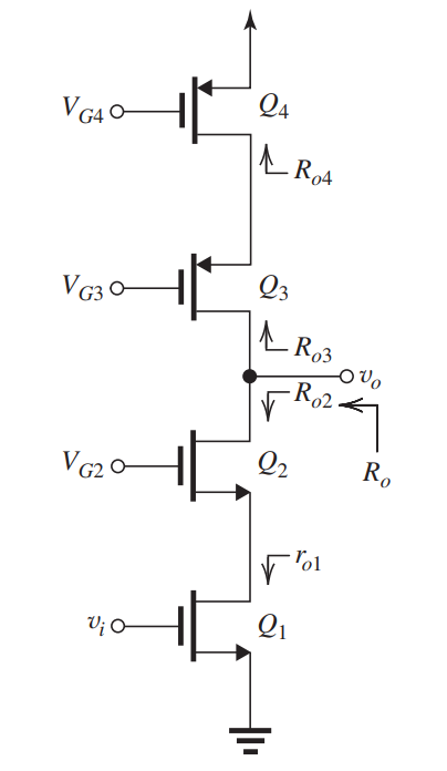
Figure 8.2.3
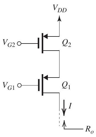 Figure 8.4.1
The cascode current source in Fig. 8.4.1 utilizes two identical PMOS transistors fabricated in a 0.18 - CMOS process for which , , and .
Design the circuit to obtain and and to allow for the maximum possible voltage swing at the output terminal of the current source. Utilize . Specify the values of and for and . As well, specify the required values of the dc bias voltages and . What is the maximum allowable voltage at the output?
Figure 8.4.1
The cascode current source in Fig. 8.4.1 utilizes two identical PMOS transistors fabricated in a 0.18 - CMOS process for which , , and .
Design the circuit to obtain and and to allow for the maximum possible voltage swing at the output terminal of the current source. Utilize . Specify the values of and for and . As well, specify the required values of the dc bias voltages and . What is the maximum allowable voltage at the output?
Free
(Essay)
4.9/5 (35)
Correct Answer:Verified
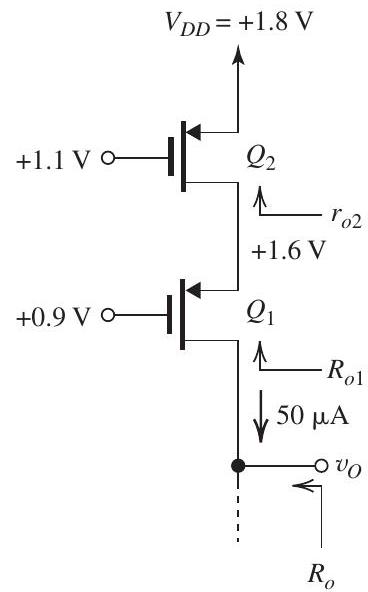
Figure 8.4.2
Minimum required voltage .
From Fig. 8.4.2, we see that
where
For ,
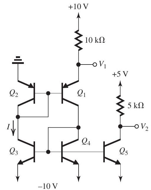 Figure 8.1.1
For the circuit shown in Fig. 8.1.1, assume and are perfectly matched, and , and are perfectly matched. Also, assume all transistors have very high and . Find , and .
Figure 8.1.1
For the circuit shown in Fig. 8.1.1, assume and are perfectly matched, and , and are perfectly matched. Also, assume all transistors have very high and . Find , and .
Free
(Essay)
4.8/5 (33)
Correct Answer:Verified
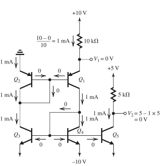
Figure 8.1.2
The analysis is shown on Fig. 8.1.2.
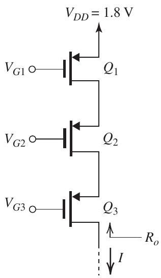 Figure 8.3.1
Design the double-cascode current source shown in Fig. 8.3.1 to provide and the largest possible signal swing at the output; that is, design for the minimum allowable voltage across each transistor. The CMOS fabrication process available has , and . Use devices with , and operate at .
(a) Specify , and .
(b) Find the ratios of the transistors.
(c) What is the value of achieved?
(d) What is the maximum allowable voltage at the current-source output?
(e) If this current source is used as the load of an NMOS double-cascode amplifier having a shortcircuit transconductance of and an output resistance equal to of the current source, what voltage gain is obtained?
Figure 8.3.1
Design the double-cascode current source shown in Fig. 8.3.1 to provide and the largest possible signal swing at the output; that is, design for the minimum allowable voltage across each transistor. The CMOS fabrication process available has , and . Use devices with , and operate at .
(a) Specify , and .
(b) Find the ratios of the transistors.
(c) What is the value of achieved?
(d) What is the maximum allowable voltage at the current-source output?
(e) If this current source is used as the load of an NMOS double-cascode amplifier having a shortcircuit transconductance of and an output resistance equal to of the current source, what voltage gain is obtained?
(Essay)
4.8/5 (37)
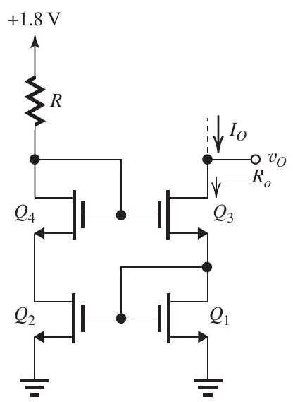 Figure 8.5.1
The modified Wilson current mirror of Fig. 8.5.1 utilizes four matched transistors for which , and . It is required to design the circuit so that with all transistors operating at .
(a) Find the required value of .
(b) Find the required value of the ratio for each of the four transistors.
(c) Find the value of the output resistance .
(d) What is the minimum voltage permitted at the output?
Figure 8.5.1
The modified Wilson current mirror of Fig. 8.5.1 utilizes four matched transistors for which , and . It is required to design the circuit so that with all transistors operating at .
(a) Find the required value of .
(b) Find the required value of the ratio for each of the four transistors.
(c) Find the value of the output resistance .
(d) What is the minimum voltage permitted at the output?
(Essay)
4.8/5 (41)
Filters
- Essay(0)
- Multiple Choice(0)
- Short Answer(0)
- True False(0)
- Matching(0)