Exam 16: Regulators, Filters, and Op-Amps
Exam 1: Quantities and Units31 Questions
Exam 2: Voltage, Current, and Resistance69 Questions
Exam 3: Ohms Law, Energy, and Power64 Questions
Exam 4: Series Circuits64 Questions
Exam 5: Parallel Circuits62 Questions
Exam 6: Series-Parallel Circuits71 Questions
Exam 7: Magnetism and Electromagnetism66 Questions
Exam 8: Introduction to Alternating Current and Voltage66 Questions
Exam 9: Capacitors66 Questions
Exam 10: Rc Circuits65 Questions
Exam 11: Inductors62 Questions
Exam 12: Rl Circuits64 Questions
Exam 13: Rlc Circuits and Resonance68 Questions
Exam 14: Time Response of Reactive Circuits65 Questions
Exam 15: Transformers65 Questions
Exam 16: Regulators, Filters, and Op-Amps307 Questions
Exam 17: Understanding Transducers, Sensors, and Conversion in Industrial Processes80 Questions
Select questions type
The arrowhead in the schematic symbol for a diode represents:
(Multiple Choice)
4.7/5  (32)
(32)
Which one of these characteristics do an op-amp and a MOSFET have in common?
(Multiple Choice)
4.8/5 (43)
The ideal amplifier has infinite gain, infinite input impedance, and zero output impedance.
(True/False)
4.9/5 (43)
The general characteristics of a common-emitter amplifier are low voltage gain, low current gain and very high power gain.
(True/False)
4.9/5 (31)
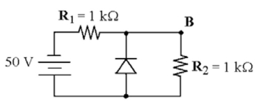
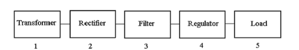 -Which block Will smooth out the pulsating dc in Figure 16-2?
(Multiple Choice)
4.9/5 (36)
PhotodiodesW ill conduct more as the light intensity upon them increases.
(True/False)
4.8/5 (36)
 -The circuit in Figure 17-5 is known as a ________ oscillator because it has a ________ coil.
(Multiple Choice)
4.9/5 (32)
 -If the BJT's collector opens internally in Figure 17-4, VB_________
(Multiple Choice)
4.7/5 (26)
 -If VIN=70 VP in Figure 19-3, the output voltage at fCO equals______
(Multiple Choice)
4.9/5 (36)
(a)
 (b)
(b)
 (c)
(c)
 Figure
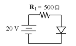
-If the diode is silicon,W hat is the voltage across the resistor in Figure 16-1(a)?
Figure
-If the diode is silicon,W hat is the voltage across the resistor in Figure 16-1(a)?
(Multiple Choice)
4.7/5 (30)
For normal operation of a NPN transistor, the base must be_________________
(Multiple Choice)
4.9/5 (33)
(a)
(b)
(c)
Figure
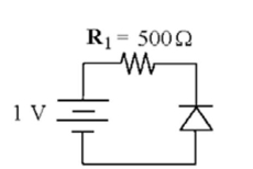
-If the polarity of the silicon diode is reversed in Figure 16-1(c), VR2 is ________.
(Multiple Choice)
4.9/5 (40)
Filters
- Essay(0)
- Multiple Choice(0)
- Short Answer(0)
- True False(0)
- Matching(0)