Exam 41: Conduction of Electricity in Solids
Exam 1: Measurement37 Questions
Exam 2: Motion Along a Straight Line90 Questions
Exam 3: Vectors43 Questions
Exam 4: Motion in Two and Three Dimensions56 Questions
Exam 5: Force and Motion73 Questions
Exam 6: Force and Motion74 Questions
Exam 7: Kinetic Energy and Work73 Questions
Exam 8: Potential Energy and Conservation of Energy65 Questions
Exam 9: Center of Mass and Linear Momentum99 Questions
Exam 10: Rotation102 Questions
Exam 11: Rolling, Torque, and Angular Momentum67 Questions
Exam 12: Equilibrium and Elasticity57 Questions
Exam 13: Gravitation61 Questions
Exam 14: Fluids91 Questions
Exam 15: Oscillations80 Questions
Exam 16: Waves83 Questions
Exam 17: Waves72 Questions
Exam 18: Temperature, Heat, and the First Law of Thermodynamics96 Questions
Exam 19: The Kinetic Theory of Gases114 Questions
Exam 20: Entropy and the Second Law of Thermodynamics61 Questions
Exam 21: Coulombs Law52 Questions
Exam 22: Electric Fields55 Questions
Exam 23: Gauss Law44 Questions
Exam 24: Electric Potential55 Questions
Exam 25: Capacitance61 Questions
Exam 26: Current and Resistance55 Questions
Exam 27: Circuits75 Questions
Exam 28: Magnetic Fields53 Questions
Exam 29: Magnetic Fields Due to Currents49 Questions
Exam 30: Induction and Inductance90 Questions
Exam 31: Electromagnetic Oscillations and Alternating Current89 Questions
Exam 32: Maxwells Equations; Magnetism of Matter87 Questions
Exam 33: Electromagnetic Waves83 Questions
Exam 34: Images79 Questions
Exam 35: Interference 147 Questions
Exam 36: Diffraction77 Questions
Exam 37: Relativity69 Questions
Exam 38: Photons and Matter Waves59 Questions
Exam 39: More About Matter Waves45 Questions
Exam 40: All About Atoms79 Questions
Exam 41: Conduction of Electricity in Solids51 Questions
Exam 42: Energy From the Nucleus50 Questions
Exam 43: Quarks, Leptons, and the Big Bang59 Questions
Select questions type
Compared to the number of conduction electrons in pure silicon, the number of conduction electrons in doped silicon is:
(Multiple Choice)
4.8/5  (43)
(43)
Compared to an insulator, the energy gap of a semiconductor is:
(Multiple Choice)
4.7/5 (36)
If ρm is the mass density of a conducting material, V its volume, M its molar mass, and NA Avogadro's number, the number density n of conduction electrons in the material is given by:
(Multiple Choice)
5.0/5 (47)
At room temperature, kT is about 0.0259 eV.The probability that a state 0.50 eV above the Fermi level is occupied at room temperature is:
(Multiple Choice)
4.8/5 (44)
A donor replacement atom in silicon might have ______ electrons in its outer shell.
(Multiple Choice)
4.8/5 (39)
Which of the following is NOT true when a back bias is applied to a p-n junction?
(Multiple Choice)
4.9/5 (41)
At T = 0 K the probability that a state 0.50 eV below the Fermi level is occupied is:
(Multiple Choice)
4.9/5 (39)
For a metal at room temperature the temperature coefficient of resistivity is determined primarily by:
(Multiple Choice)
5.0/5 (36)
Which one of the following statements concerning electron energy bands in solids is true?
(Multiple Choice)
4.9/5 (41)
Electrons in a full band do not contribute to the current when an electric field exists in a solid because:
(Multiple Choice)
4.8/5 (34)
If E0 and ET are the average energies of the "free" electrons in a metal at 0 K and room temperature respectively, then the ratio ET/E0 is approximately:
(Multiple Choice)
4.8/5 (43)
When a forward bias is applied to a p-n junction the concentration of electrons on the p side:
(Multiple Choice)
4.9/5 (47)
Switch S is closed to apply a potential difference V across a p-n junction as shown.Relative to the energy levels of the n-type material, with the switch open, the electron levels of the p-type material are: 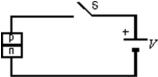
(Multiple Choice)
4.8/5 (22)
At room temperature, kT is about 0.0259 eV.The probability that a state 0.50 eV below the Fermi level is unoccupied at room temperature is:
(Multiple Choice)
4.8/5 (37)
For an unbiased p-n junction, the energy at the bottom of the conduction band on the n side is:
(Multiple Choice)
4.8/5 (31)
At T = 0 K the probability that a state 0.50 eV above the Fermi level is occupied is:
(Multiple Choice)
4.9/5 (40)
Filters
- Essay(0)
- Multiple Choice(0)
- Short Answer(0)
- True False(0)
- Matching(0)